Tutorial: Introduction to PCB design with KiCad version 5.1 (Getting Started)

Introduction to PCB design with KiCad version 5.1

In this tutorial we will learn the very basics of using KiCad for designing a circuit board. It is assumed that you already installed KiCad. If not head over to KiCads download page and follow the instructions for your operating system.

This tutorial is split into the following sections:


What is needed for a PCB to be produced?

A Printed Circuit Board (PCB) is defined by a number of layers. These layers include a defined number of copper layers, solder-mask, silkscreen and board edge which are required by the board house to manufacture your board. Additional layers like the fabrication and courtyard layers are there to document your board or help with ensuring manufacturing constrains are met.

The PCB Layout software uses footprints that define the interface with every component. Pads in a footprint define the places where the leads are soldered to by defining a copper geometry, soldermask cutout, paste stencil cutout and if necessary a drill hit. Graphics on technical layers help for documentation like silkscreen. And graphics on the courtyard layers ensure that no other component is placed to close.

To define which pads need to be connected with traces (or other means) you use the connectivity information that you get from the schematic. This connectivity information is also called a net-list (it is a list of nets plus defines which pad is assigned to which of these nets).

The schematic is build up from symbols that are the abstract view of the function of every component (The schematic is then the abstract view of the systems intended function) Symbols define pins that are mapped to footprint pads (via the pin/pad numbers and the footprint field of the symbol). You define the connectivity information by using wires that are used to connect pins together. (or you can also use labels or power symbols)

A schematic can additionally contain information for creating a bill of materials. This information is contained in additional symbol fields.

The design flow

The design process goes the other way round than this introduction. One starts with an abstract idea for the system (your customers specification, your own idea about what you want to achieve, …)

This specification is then converted to a schematic view of the solution to the given problem. Part of the schematic design is to select the components that you use for making the system. (In this step you need to ensure that you can buy the required parts.)

The schematic is used to define the connectivity of the layout. In the layout tool you then finally define the layers required by the board house by using footprints and the connectivity information that is used to define the copper layers.

The tutorial here does not go into details how to get from the abstract idea to the schematic nor do we show how to select components. It shows you how to use KiCad to get from this known information to the final product.

9 Likes

Creating a Project

A KiCad project is a combination of multiple files that describe your printed circuit board (PCB). There will be at least one schematic file that describes the function of the PCB. It uses symbols, wires and labels to achieve this. This file is used to generate the connectivity information for the layout as well as defining which footprints will be used.


To create such a project we need to start KiCad like you would any other program.
The main window of KiCad will open. It is used to handle tasks at the project level. Use it to create or open projects and to open the tools responsible to edit project files.

Create a new project using File->New->Project (or shortcut crtl+n).

An operating system dependent file browser like tool will open. With this tool navigate to some place to store your project and enter the project name (example: first_pcb) in the input field. Create the project by selecting “save” (or the equivalent for your operating system).
New_Project

The result will look something like this

2 Likes

The Schematic

In this section we will make a schematic using only simple symbols and wires. You will learn one way of how to assign footprints to the schematic as this is required to start the layout.

Starting the editor

Open the schematic editor (EESchema) by clicking on the button for the schematic layout editor (leftmost of the large buttons. See screenshot)

If this is the first time you open EESchema then a window will pop up asking you how you want your libraries setup. Accept the default option. If the default option is not available then you somehow did not install libraries with KiCad. No worries this can be solved
EESchema%20--%20Init_Lib_Table

An empty schematic will open for you. I have annotated the important parts of EESchema in the screenshot such that you know how i refer to the different parts of EESchema. In this tutorial we will mostly use tools from the right and top toolbar. All KiCad tools are reachable via hotkeys and we will make use of them (I generally have one hand on the keyboard at all times as i make heavy use of the hotkeys).

Zooming and Panning

First familiarize yourself with the basic interactions of EESchema. Use the mousewheel to zoom. The middle mouse button is used to pan. The default zoom behavior might need a bit getting used to as it centers your view around where the cursor currently is. This is a very powerful feature that allows very efficient navigation of the canvas. If you however find it is too disorientating then you can turn it off in the preferences dialog (Menu bar: preferences -> preferences -> Common -> Center and Warp on zoom)

Add Symbols

With that gotten out of the way lets start making our schematic. We will make a simple non inverting amplifier with the LM321 and a few connectors as the interface. Use the add symbol button Button_add_symbol in the right toolbar (or “place->symbol”) to start the symbol mode. A similar button is in the top toolbar but that one opens the symbol editor.

After that click somewhere on the canvas and the add symbol dialog will come up. Enter LM321 into the filter field and select the symbol from the result by single clicking. You will now see a preview of the symbol and symbol details in the dialog. Double click on the symbol name or click ok to add the symbol to the schematic.

Now the symbol should be attached to your courser. Move it around a bit to get a feel for this. Then place it down somewhere in the middle of the drawing area by left clicking. In the end your canvas should look something like this.

While you are in the add symbol mode you can call the add symbol dialog again with a simple left click. We do just that and add a resistor (R) and a connector (Conn_01x02).

I suggest you use the filter field (the one wher you entered LM321) to find these symbols and get a feel for how it works. For the resistor the searchterm resistor will get you the resistor but not as the only nor first result. But if you observe the results while typing you will notice that the correct symbol does come up after typing r (counterintuifely getting more specific with the search term in this case results in a less useful result – This is admittetly a weird quirk of kicad but well so be it.).

As a further hint: all basic symbols are found in the device lib. Connector symbols are in the connector_generic lib (the connector lib has more specific connector symbols like the ones for a usb connector). It might pay to just look through the libraries in general to get a feeling for what to expect where. And remember everything about the official library including its organization are documented in the library convention https://klc.kicad.org/

Look at the screenshot to see where i added mine. When you added both of them use the ESC key to end the add symbol mode.

Copy Symbols

We now need one more resistor and two additional connectors. We could add them in the same way as we did before but why not simply copy the things we already have. Hover over the resistor you placed and use the hotkey c to copy it (alternatively also reachable via the right click context menu). The copy will be attached to your cursor so place the new resistor just below the first one. Repeat this for the connector until your schematic looks something like this.

Move, Rotate and Mirror Symbols

The rightmost connector is facing away from the amplifier, so we want to rotate it. This is done by hovering over the connector and pressing the hotkey r. You can also mirror the symbol using x or y. Moving it around is done with m. Play around with these 4 hotkeys as you will need them when you start your real projects. You can even use the other 3 hotkeys while you move your symbol around (while it is attached to the cursor). All of these actions are also available via the right click context menu of the connector (handy if you ever forget the hotkeys).
After you played around a bit, place the symbols such that they look something like this.

Make the Connections

If you look at your symbols you will see that they have lines sticking out of them with a small circle at the end. The lines are called pins and the circle indicates that this pin is not connected. We will use wires to create the connections required. For that start the wire tool found in the right toolbar Button_wire .

Like with the add symbol tool nothing happens at this point in time. Move your mouse over the end of the output pin of the amplifier (The one at the tip of the triangle. The end of the pin is what is marked with the circle.) Use left click to start the wire. If you now move the mouse around then you will discover that a green line is following you. Move the mouse to the nearest pin of the nearest resistor and click again to end the wire at this point. The schematic should now look like this.

Now also connect pin 2 of the connector to the amplifiers output pin. (First click on the connector pin and then on the output pin. The output pin no longer has a circle but you can identify the end of it as it is where the other wire already connects.) KiCad will now add a circle where the old wire and the new wire cross. This circle is called a junction dot.

Now connect the rest up as shown in the following screenshot. Notice that we leave the V- pin of the amplifier unconnected for now. You can add additional direction changes while in the wire tool by left clicking where you want this corner. I used this for the connection of V+ to the connector (to get more space for the text above the other connector.) You can start or end a wire anywhere on another wire also by left clicking. A new junction dot should then be generated there as well.

We now only need to connect the V- pin to the wire representing our low voltage potential (The horizontal line on the bottom of the schematic.) There is however no way to do this without crossing some other existing wire (or worse going through a symbol). This is not a problem and will happen in nearly every schematic you ever make. Click on the pin and then on that wire. If you do it right then no junction dot should appear in the wire connecting to the - pin of the amplifier.

Check Connections with the Highlight tool

Now that we made a few connections we might want to double check what is connected. First lets double check that the last wire we just added really is not connected to the feedback connection. Activate the highlight net tool Button_highlight and left click on that wire. The result should look like the screenshot. To get rid of the highlight click anywhere on the canvas (where there is no wire).

Get Ready for the Layout

Add Annotation

Symbols in schematics are identified with a so called reference designator. There are different styles how this is done (= lot of competing standars) but most such styles use a combination of letters representing a group of components followed by a number. The KiCad standard library is configured to follow a common rule that is not really codified in an official standard. KiCad however has a restriction that any reference must end in a number.

At this point our reference designators still have question marks in them. Which means they have not yet been annotated. We use the annotate button Button_annotate in the top toolbar to start the annotation dialog (alternative: Menu bar: Tools->Annotate Schematic…). We do not need anything special so just accept the default and press annotate. If everything seems ok press close.
annotation_dialog

Now your symbols should have gotten unique reference designators.

Assign Footprints

In this part of the tutorial we show one option how symbols get their footprints. We also have a more detailed lecture about footprint assignment
Start the assign footprint tool with the button in the top toolbar Button_assign_footprints (alternative: Menu bar: Tools->Assign Footprints…)

If you never started anything layout related before then you get a popup informing you that a default footprint library table was created. You can click ok.
cvpcb_lib-table

The assign footprint tool is split into three columns. The leftmost colum shows all libraries available. The middle column holds the symbols placed in the schematic and their assigned footprints. The rightmost column shows the filtered footprint list.

Move the assign footprint dialog to the side such that you see both the schematic and the dialog at once. Click on any row in the middle collumn of the dialog. The symbol gets hightlighted and the view is moved such that this symbol is in the center.

Notice that the amplifier (reference U1) has already a footprint assigned. This is because the symbol is setup this way in the library. Most symbols you get with KiCad are setup this way and you can typically keep this default footprint unchanged (such symbols are called fully spezified or sometimes also atomic).

Now lets assign the footprints to the remaining symbols. We set the filter options to be “Use Schematic symbol footprint filter” and “Filter footprint list by pincount”. If we now click on the first connector we should see a number of connectors listed in the right column. You assign the footprint to the selected symbol(s) by double clicking on the footprint name in the rightmost column. I suggest to use JST_EH_B2B-EH-A_1x02_P2.50mm_Vertical for J1 and JST_PH_B2B-PH-K_1x02_P2.00mm_Vertical for J2 and J3. You can assign the same footprint to multiple symbols by selecting them at the same time (crtl or shift plus left click to add to the selection)

When all footprints are assigned then we are ready to click ok.

Save your schematic with the button in the top toolbar (or crtl+s). We are done for now.

6 Likes

The Layout

You will learn how to create the board acourding to the schematics connectivity information by using traces to connect the pads of footprints. We will also look at how visibility options can be used to improve your KiCad expirience.

For convenience here the project at the stage after finishing the schematic.
first_project_schematic_done.zip (221.2 KB)

Starting the editor

Open the layout editor (Pcbnew) from the main window via the third large button.

If you open Pcbnew for the first time then a pop-up will come up asking you if you want to enable hardware accelerated graphics. You can select Enable Acceleration unless you have reason to think that your computer can not handle accelerated graphics. You can always change your mind later on.
enable_acceleration

An empty layout will open for you. I have annotated the important parts of Pcbnew in the screenshot such that you know how i refer to the different parts of Pcbnew. In this tutorial we will mostly use tools from the right and top toolbar. All KiCad tools are reachable via hotkeys and of course the menus.

Zooming and Panning

Pcbnew has the same default behaviour as EESchema so this is nothing new to somebody who already followed the schematic tutorial. Still, a reminder: Use the mouse wheel to zoom. The middle mouse button is used to pan. The default zoom behaviour might need a bit getting used to as it centers your view around where the cursor currently is. This is a very powerful feature that allows very efficient navigation of the canvas. If you however find it is too disorientating then you can turn it off in the preferences dialog (Menu bar: preferences -> preferences -> Common -> Center and Warp on zoom)

Getting the Schematic Information into Pcbnew

We need to tell KiCad that we want to get the information contained in our schematic into Pcbnew. For that use the update PCB from schematic button Button_update of the top toolbar (alternative: Menu Bar: Tools->Update PCB from Schematic…). The update dialog will pop up. We can use the default settings so press Update PCB and check that there is no error message reported. Assuming there was no error then press close. (If there is ask on the forum for help) For more details about this process see Update PCB from Schematic's match methods
update_pcb

There should now be a number of footprints attached to the cursor. You can move them around and place all of them with left click. The footprints are still selected so click anywhere in empty space or use the ESC key. Notice the colour change. Play around a bit selecting and deselecting footprints. (all done with the left mouse button). Get a feel for where you need to click to select the footprint and where you need to click to select the reference designator.
updated

If you have the schematic editor open then you can see that the corresponding symbol is highlighted similarly to when we worked with the assign footprints tool. This also works the other way round. You can select a symbol in the schematic and the corresponding footprint will be selected in the layout. (Select a symbol by left clicking on it. There is no visual feedback in the schematic but the footprint will be highlighted.)

Handling Layer and Item visibility

The view is a bit cluttered for my taste. For now, we do not need to see the values nor the silk layer. Managing layer visibility is done in the right sidebar. The meaning of layers is described in the FAQ.

Every entry in this sidebar is identified by its name to the right and has a coloured square next to it. This square shows the current colour of that entry and can also be used to change the colour by double clicking. Next to the square is the visibility checkbox. Deselect F.SilkS and observe what changes. Switch to the items tab and deselect Values. Be prepared to experiment with layer and item visibilities during your work with KiCad. Everyone has their own preferences, so I really can not give you a rule for when to use which layers.
layers_cleaned

One layer has a blue triangle next to it. This is the currently active layer. Any tool you choose will start on that layer (if the tool can work on that layer, otherwise it chooses the nearest fitting layer.) The KiCad renderer works like a stack. The active layer is rendered on top, then all other layers of the same side followed by the layers of the opposite side (So if you have any back layer active all back layers are rendered on top of the front layers.). Layers can have transparency but the default KiCad colour scheme does not use that feature. You might therefore want to look into custom colour schemes sometime later on.

Ratsnest lines

The thin white lines that connect different pad centers are called ratsnest lines (sometimes also Airwires). These show which points need to be connected to complete the circuit to the schematic’s specification. Note however that they are always drawn between the nearest points of a net that are not connected. It might not always be the case that one makes the connection following this suggestion.

Organizing the Footprint Placement

Right now the footprints are placed kind of randomly. A big part of good layouts is deciding on where to place which footprint. I find that investing time into good placement is worth it and spend typically 50% of my layout time with this task. This of course varies widely depending on number of footprints and complexity of the connections. Good placement reduces the number of ratsnest crossings and keeps parts close together that need to be close to each other.

To move a footprint select it with left click and then use hotkey m to move it and r to rotate it. You can also do this without first selecting the footprint but I find it easier to get the right thing when I first select it. Play around a bit with the location of the parts until you are happy with it. You can of course take inspiration from the screenshot below.

Movement is done with respect to the grid. It might be the case that the selected grid is a bit too coarse. Use the drop down button in the top toolbar to select the grid you want (alternatively also found in the right click context menu.) I typically use 0.5 mm grid for drawing the board outline and copper zones, 0.25 mm grid for arranging footprints and 0.05 mm for laying down traces.

The board outline

The board outline is defined using graphic elements on the edge cuts layer. The edge cut must consist of closed shapes but there can be inner cutouts defined. To get a closed shape every elements endpoint must be within 0.01 mm of the next elements point.

To draw the outline select the graphic line tool Button_graphic_line from the right toolbar. Click where you want one of your boards corners and then move the mouse to where your second corner should be. Holding the Ctrl key while doing this will enforce orthogonal lines. Click when you are happy with your second corners position and continue on to the third point. Repeat until you are back at the first point and double click to end the tool.

If you want to edit a line then select it and squares should appear at its endpoints. You can drag these endpoints but be aware that the current version of KiCad does not move the next lines endpoints as well. Complex board outlines might therefore be best made in a parametric CAD program and imported into KiCad as step or you could use freecad plus stepup

Adding traces

We can now start to add traces as the footprints are now placed in a well organized manner. Select the route tracks tool from the right toolbar Button_router . With that tool active click on pad 1 of R2. Notice how all pads hat need to be connected to this pad are now highlighted.

Now move the mouse and you will see you are followed by a trace. KiCad has a powerful semi-automatic routing engine the so-called interactive router or also push and shove router. By default, the router is in walk around mode, so I suggest you move around your mouse to anywhere on the PCB and observe what the router does.

Notice that the trace has a dark grey envelope. This is the required clearance set in the netclass. Similarly, every footprint pad has a thin line around it which also shows the clearance set in either the pad, footprint or netclass. How all of this is setup will be handled in other tutorials for now just be aware what these graphics mean.

Using this router engine will require a bit of practise to get the most out of it so for now just connect the trace that should still start with pad 1 of R2 to pad 2 of R1 by left clicking on the latter.

If you ever want to cancel a trace use the ESC key. You can help the interactive router find the route you prefer by fixing some points of a route. A left click will however not fix the current end point but the previous corner. You can also fine-tune existing traces by dragging parts of them using the hotkey d. If you do not like a trace then delete it with hotkey Entf. Now lay down the rest of the traces but play around a bit to get a feel of the different features. In the end your board could look something like the screenshot below. I placed everything on the top copper layer. Handling of different copper layers as well as copper zones will be done in the next tutorial.

Check the Board

KiCad comes with a so-called design rule check tool. This tool is used to check if the design can be produced as drawn. (assuming the rules are setup correctly.) The DRC is useful even in our case where we did not really setup the rules. At least it can check that the outline is made correctly, there is enough space between components and that we have connected everything. We can even check the clearance against KiCads default settings which are very conservative and should therefore allow any board house to manufacture our board.

To start DRC select click the button in the top toolbar Button_drc . In the dialog that opens click the list unconnected button to find out if everything is connected. If nothing is reported then you have connected everything as required by the schematic. After that click the run DRC button to see if there is any problem. If nothing is reported then you are done with this tutorial. Otherwise, use the DRC message and the placed marker to find out what to do. You can also ask for help on the forum.

Inspect the Board in 3D

KiCad includes a 3d viewer. Some of the footprints shipped with kicad come with 3d models. In this particular case all used footprints have a 3d model. The 3d viewer is found under them menu bar entry view -> 3d view or hotkey alt+3.

Save the layout, we are done with this section of the tutorial.

5 Likes

Improve the Schematic

We previously made a simple schematic using only symbols and wires. Now it is time to add more powerful features like power symbols and labels to the mix. We will further look at the handling of multi unit symbols.
As a convenience here the project as it would be so far: first_project_pcb_done.zip (223.4 KB)

Multi Unit Symbols

KiCad can split complex symbols into smaller units that can be placed independently. This feature is called a multi unit symbol. I selected the AD8676 dual OPA as a replacement for our LM321. The AD8676 symbol is split into three units. One for the power supply pins and two for the two OPA units.
First delete the LM321 from the schematic to make place for the new symbol. Use the ‘Del’ key while your mouse is above the symbol.
Now open the add symbol dialog with hotkey a. You do not need to click as this hotkey triggers an immediate action. Use AD8676 as the search string and expand the collapsed library and symbol (The library is collapsed because of a bug when finding only a single multi unit symbol)

Place Unit A where the LM321 was. Place unit B somewhere to the side and place unit C above unit A such that its pins reconnect with the original LM321 power connections. KiCad remembers recently added symbols so you do not need to enter the filter string again. Just expand the virtual recently added library in the symbol chooser and select what you need.

In the end the Schematic might look something like this

Connections Without Wires (Power Symbols and Labels)

KiCad has 3 ways to make connections without needing to draw a wire.

  • Global labels: two (or more) labels with the same name are connected no matter on which sheet they are.
  • Power symbols: These are special symbols that work as a global label
  • Local labels: two (or more) local labels are connected if they are on the same sheet.

There is also a fourths type of label, the hierarchical label. This label is special as it is used to define the interface of a hierarchical sheet. See: Hierarchical or flat schematic design, what is best for me? (How to deal with multi page schematics?)

The following picture shows the 3 label types next to their respective buttons that add them. As with a pin or wire the thin square marker shows where you can connect something to the.
Screenshot from 2021-01-13 22-45-31

Our schematic is a single sheet schematic so the label type does not really matter. We will use power symbols and local labels to show how they work.

First notice that our V- connection is a bit messy with that many things connected by a wire. Let’s clean this up a bit by using the power symbol GND. Using a named net has the added benefit that we can use copper zones in our next iteration of the PCB. To do this we first delete all connections of this single net. Then use the add power symbol button button_power (or hotkey p) to get the add power symbol dialog. Select GND (with the help of filtering) from this dialog.

Place it near every pin that needs to be connected with the V- pin of the OPA and connect the symbol to the pins with short wires. The short wires are needed to allow the highlight tool to work as it only highlights wires not symbols or labels.

Now we remove the wire connecting V+ to the connector and replace it with a local label to show how that works. (Normally one would use another power symbol to connect this.) Adding a local label is done by activating the label tool in the right toolbar button_local_label . Click somewhere on the canvas and use V+ as the label name. Place one such label near the connector pin and one near the V+ pin of the OPA.
local_label

Connect the labels with short wires to their respective pins.

You can now use the highlight tool again to check if everything is still connected as you expect.

Cleanup the Schematic

Right now the schematic looks a bit messy. The Reference and value fields of your symbols overlap with wires or other symbols. The fields can be moved separately from their symbols with hotkey m and rotated with hotkey r.
Move the fields around until you are happy that your schematic looks clean.

Sometimes its necessary to move symbols around to get a clean schematic. You might not want to break the connection between the symbol and its wires with such an operation. The grab tool (hotkey g) exists to fulfil this usecase. Grab any of the symbols with g and observe what happens if you move the mouse around. Compare this to using hotkey m. The hotkey g can also be used on wires and junctions. Yet another thing you might want to experiment with.

Electrical Rule Check

KiCad includes an electrical rule checker (ERC). This is a net based system that checks the electrical types of all pins connected to each other. Every type has a set of pin types it can be connected with and others that result in an error or warning. This error matrix can be changed by the user I would however suggest keeping it as is.

We need to first annotate the schematic as ERC only works on fully annotated ones. So run the annotation tool again. To open the ERC dialog click the button button_erc in the top toolbar. In the dialog click run. We will get quite a few reports. Arrows are added to the schematic to point to the places where KiCad found the error. Every report contains a link to the arrow so click on them and observe what happens.

The 3 pins of unit B are easy to explain and easy to fix. We simply never connected something to them so ERC complains. We simply place no connection flags button_nc to make ERC happy and to show that tool for the purpose of this tutorial. (Normally one would not want unconnected input pins.)

The remaining two errors are harder to explain. Especially as we were “lucky” and triggered two different bugs (wrong pin reported, power symbols should have low priority).

The power supply pins of the OPA should be the source of the error in both cases. These pins are defined as power input pins. Every power input pin must be connected to a power output pin for ERC to know that this pin is correctly supplied.

We supply our board via a generic connector symbol. This symbol does not define its pins as power output. There is a special symbol in the power library that takes care of telling ERC that the net is supplied. This symbol is called PWR_FLAG. Place one near both of the pins of J1 and connect them to the pins. More details see: ErrType(3): Pin connected to some others pins but no pin to drive it
pwr_flag

If we now run ERC again it will come out clean.

Save the schematic again we are done with this section of the tutorial.

5 Likes

Improving the Layout

We did only use traces to define the connectivity in the first round. We still have a full second copper layer that we never used. So lets introduce copper zones and vias to the mix. You will additionally learn how you get changes made in the schematic back into the layout and will also learn how to change the unit used in a schematic to allow for easier connections.

We continue with the previous result. For convenience here the project as it would look like first_project_schematic_done.zip (221.2 KB)

Updating the PCB with the new OPA

We changed the OPA in the schematic to one that does not use the same footprint. Now we need to get that into Pcbnew. Open the update PCB from schematic tool again (top toolbar or tools menu). Activate Exchange footprints and Delete extra footprints.
update_pcb

After clicking update and close you should have the new footprint attached to the mouse and the old one should be gone. I place the new footprint somewhere to the side as i first need to clean up the traces that are now left from the old footprint. This would be beneficial if the new footprint would be similar to the old one but in this case we will simply delete the unwanted traces.
updated

Cleanup Traces

We use the cleanup tracks and vias tool from the edit menu to get rid of the unnecessary traces. In a real project you would probably be a bit more precise than using this tool for the current task. In a small project like the one we have now it would even be ok to just delete everything and start over from scratch.
cleanup_dialog

Selection Options for Traces

We want to move the current ground connections to a copper zone on the bottom layer, so we delete all GND tracks. Right click on one section of the GND net -> select -> all tracks on net (in our case all connected tracks yields the same result.) I would suggest you play around a bit with different selection options, especially with the single track selection option. Try it on different places of the GND net and observe which parts get selected.


Now we can use the Del key to delete the selected traces (select the full GND net again if you played around with other selection options).

Component Placement and Unit Exchange

In my example I will need to move J1 out of the way to get The new OPA in. But even if I do that there is not really an orientation that I can place the new OPA in that would yield in nice orderly ratsnest lines.
I could of course rip up more of the existing layout but there is an easier solution. Our new OPA has two units in it. Go back to the schematic and exchange the unit. Right click on U1A -> Properties -> Unit -> Unit B. Do the same with the old U1B (does not happen automatically) and change it to unit A.
This is something you will quite often do in larger projects. Especially if you interface with a configurable component like a microcontroller. In a lot of cases it makes more sense to exchange pins or full units in the schematic (and therefore the embedded software) instead of compromising the layout. PCB design can be seen as an iterative process.


Don’t forget to run ERC again after such a change. Then update the PCB from schematic. We can now easily place the OPA such that it can be reconnected with the rest of the layout.

Changing the board outline

The board outline needs correcting in my current layout. As a first step move the top line up until it does no longer interfere with J1. Use the move command (hotkey m) ot achieve this. I suggest doing this zoomed in as selecting lines is tricky when zoomed out.

Next we need to lengthen the two other lines. Left click one of them to get the squares on the end. Drag that square to close the outline and repeat on the other line.


Copper zones (GND plane)

Copper zones are a useful tool used to make power planes or just large copper areas in general. I will show the basics of using it, for more details head over to the FAQ article How to create a power plane (using zones).

To add a copper zone select the zone tool from the right toolbar button_zone . Click where you want one of the zone corners to end up (Example the top left corner of the board outline). The zone properties dialog will now open. In it, we select B.Cu as the layer and GND as the net. We keep everything else on default for this tutorial. This will most likely not be the case in most of your projects so always check all settings carefully against your requirements. Zone properties can also be changed later by right clicking on the zone outline and selecting the properties dialog from the context menu.

When you close the zone properties dialog you will discover that a thick white line follows your mouse again.

Click where you want the next corner of your zone (example the next corner of the board outline) and repeat that until you have only one corner left before you would come back to the start. At this last point do not single click but double click to end the tool and create the zone. (You could also single click now and then double click on the first corner. Both result in the same outline.)

Zone visibility

Copper zones are quite intrusive. It gets very hard to see what else is going on with such large areas filled in one colour. I tent to show zones in outline mode while i work on the project and only set it back to fill mode from time to time to make sure that everything is still ok.

Zone visibility options are found in the left toolbar. Play around with them to get a feel what type of visiblity you prefer. This is again something where you might want different visibilites for different tasks so switch it around if needed.

Vias for Connecting GND pads.

The copper zone is on the bottom layer. We however have a few surface mount pads on the top layer that require connection to GND. We could connect every such pad to the nearest through hole pad but why even bother with zones in that case? So lets add a few vias. Activate the routing tool (hotkey x). Click on pad 2 of R2 (The GND pad of R2). Press v to add a via to your cursor and move your mouse around. Notice that you know have a via at the cursor which is followed by a trace back to your starting position. Also notice that the active layer is now the bottom layer (if the zone would be shown in filled mode then you would now be blind).

I suggest to place the via by left clicking slightly outside the pad it originated from. (KiCad allows to place vias inside pads but it might create problems in your manufacturing process. Check with your assembly guys to discover if this is a problem.)

Repeat the same for the remaining ground pad of the OPA. You do not need to manually switch the layer as clicking on the pad will bring you to the correct layer. This would be different for through hole pads as every layer is valid for them.

Finish the Layout

Now just connect the remaining traces as in the previous tutorial. After that run DRC and ensure everything is ok. You can again view the PCB in the 3d viewer to possibly get a better understanding of the geometry.

Other visibility modes

The left toolbar also has visibility options for vias, traces and pads in addition to the previously shown zone fill modes. All these objects can be shown in outline mode or in filled mode. Play with them to see what happens (you might need them or accidentally press them at some point so it pays off to understand how they work)

Another useful visibility mode is the high contrast mode. It desaturates all layers except the active one.

Note: Both visibility demo pictures are stitched together in a graphic program. The visibility buttons will change the full view!

We are done for now so save your project.

4 Likes

Getting the PCB Ready for Manufacturing

We continue our work so for your convenience here the project files you should have so far: first_project_pcb2.zip (8.5 KB)

We have not really looked at the requirements for manufacturing this board until now. For example, we used the KiCad default rules instead of defining them based on our manufacturers capabilities. Nor did we define our own electrical requirements.

In a typical project you will start with first defining these rules. We show this here at the end as it is a more advanced topic that requires all the knowledge you got so far.

What Influences the Design Rules?

There are two major influences to your design rules. The manufacturers capabilities define absolute limits and your own design requirements can define other limits (not violating the absolute limits).

Where do I get the Rules for my Manufacturer?

Every manufacturer has a set of rules that depend on their manufacturing capabilities. These rules map their manufacturing tolerances to board feature sizes and clearances. Typically, such definitions are found on the manufacturers website. If they are not found there then you might need to ask for them by mail.

Be aware that the design rules can differ greatly between different manufacturers and also between different options of the same manufacturer. (For example the copper layer thickness can influence the minimum soldermask to copper clearance for pads.)

A manufacturers spec sheet could look similar to the table below. (Reduced spec sheet showing only the things we care about for this tutorial. I do not name the manufacturer here as i do not want to show any bias.)

Specification <20µm Cu 21 … 35µm Cu 36 … 45µm Cu
Clearance Pad to Pad 50µm 75µm 90µm
Clearance Track to Pad 50µm 75µm 90µm
Clearance Track to Track 50µm 75µm 90µm
Minimum Track Width 50µm 75µm 90µm
Minimum Mask Land Width 45µm 45µm 60µm
Minimum Mask cutout to trace 50µm 50µm 50µm
Minimum Mask clearance 50µm 50µm 50µm
Clearance Drill to Copper 0.2mm 0.2mm 0.2mm
Minimum copper restring 250µm/100µm 250µm/100µm 250µm/100µm
Minimum Drill 0.2mm 0.2mm 0.2mm

The particular manufacturer I looked at had a contradiction for the copper restring within their ruleset. I needed to contact them to get clarification about that. Be prepared that this can also happen with your manufacturer (The reasoning behind the contradiction was that they have two different drill processes with differing tolerances. I could have selected the option with the tighter tolerances which would have resulted in a smaller restring but it would have cost a bit more and the delivery time would have increased.)

Other Sources for Design Rules

In addition to manufacturing constrains you can also have electrical constrains. One such example is defining a trace width larger than the manufactuers suggestion for high current traces to limit voltage drop. The inbuild track width calculators (found in the PCB calculator tool of the main window) can be used to determine these requirements. Or you can use an online tool of your choice.

Another parameter can be a larger copper to copper clearance required for high voltage designs. Here you will most likely need to follow an industry standard or government regulations.

We will require the GND and V+ net to have a minimum width of 0.4mm and a clearance of 0.2mm for the purpose of this tutorial (No real reason, just to show how it is done)

Design Rules in KiCad

Until now, we used the default settings for the design rules. KiCad currently has a bare minimum DRC system. This makes it easy to define the rules but limits what can be done. (Future versions will be more powerful and therefore also more complex.)

From Pcbnew start the board setup dialog found in the file menu (File->Board setup). This dialog is split between a tree view of the possible settings pages to the left and the settings input view. Of note in this tool is that every entry in the tree view defines settings (Even the top layer!)

Settings Page “Design Rules”

This page defines the absolute limits for PCB features which includes the minimum track width as well as minimum sizes for vias and their drills. The same page is also responsible for enabling advanced (more expensive to produce) vias.

We need to map the given manufactuer values to the respective settings here:

  • minimum track with is given directly as 75µm=0.075mm
  • minimum via drill from the minimum drill size 0.2mm
  • minimum via diameter from the drill size and required restring: 0.2+2*0.25 = 0.7mm

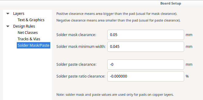
Settings Page “Solder Paste/Mask”

This page defines the clearances between copper pads and the mask or paste layer. Both of these settings can be overwritten within the footprint or pad settings.

We can encode only the soldermask clearance and soldermask minimum width setting given by the manufacturer. The distance between mask and trace can not be encoded here, it needs to be respected within the net clearances.
The paste clearances will depend on the stencil manufacturer. We leave them at the default values for this tutorial.

maks

Settings Page “Net Classes”

We first setup the default net class to the manufacturer minimum requirements. We set the track width to 0.075mm and the clearance to 0.1mm. We could set the clearance to 0.75mm but then we do violate the mask to trace requirement given by the manufacturer. (We can sadly not give a separate definition between mask cutout and trace)
The via sizes are setup to the minimum (0.2mm drill, 0.7mm size)

We use the plus button to add a new net class. Name it “Supply” and set it up with 0.4mm trace width and 0.2mm clearance (as we imagined we would require for our system)
We also need to assign this net class to our supply nets. For that select the Supply net class in the assign net class drop down menu. Then select the GND and V+ nets in the net lists and use the assign to selected nets button to get the nets into the supply net class.

Updating the pcb with the new limits

Make sure you set the values as shown previously and use the OK button to save the board settings.

We now need to update the board (again) as we changed the trace widths and clearances of all nets. (This is why one normally does this up front.)

Use block select to select everything. Then right click -> select -> filter selection and activate only vias and tracks.

sel-filter-dialog

After that only tracks and vias are selected. Trigger the properties dialog (hotkey “e” or from the right click context menu) which allows manipulating all selected traces and vias at the same time. Select “by netclass” for both the track width and via sizes and press OK.

We now also run DRC to check if everything is ok. I got an error for the V+ trace being too close to pad 1. You might get a different result depending on how exactly you layed out the traces in the last section.

I fix that by dragging the affected track segment away from the pad. What you need to do will possibly differ but will also most likely mean you need to move around traces.


Notice that 0.075mm traces are very thin. We would have enough space to keep them larger. It is suggested that one does not go to the absolute minimum sizes required by the manufacturer unless it is necessary. You can change the netclass again if you want to have additional practice. Otherwise, just leave it as is.

Generating Gerber Files

The final step left is to generate gerber files and sent them to your manufacturer. Some manufacturers provide a web upload for gerber files while others require you to send a mail.

In KiCad gerber output is found via the plot entry in the file menu or via the button button-plot in the top toolbar.

In the layers list select the layers you want to have included. In our case the default selection is ok. If you do not plan to have a solder paste stencil manufactured then you can deselect the paste layers.
All other settings highly depend on your manufacturer and your personal preferences. For this tutorial we leave everything as default.

The only thing we do is select a different output directory. Click the folder button to open a file browser like tool and create a folder “gerber” within your project directory. The tool will ask if you want this path to be relative which we suggest you accept. Clicking plot will generate the gerbers as specified.

We now only need to generate the drill files. Click the generate drill files button. All of these settings again depend on your manufacturers requirement, so we can not really give you a step by step explanation. For this tutorial we again keep everything as default and click the generate drill file button.

Likely Gerber Parameter Changes for your Manufacturer

The main parameters which differ between manufactuers are:

  • Some manufactuers require the so called protel file naming scheme
  • Some manufacturers require the plated and non plated drill definition files to be combined
  • Zero formats can be different and selecting the wrong one might explain error messages
  • Some manufacturers suggest one sets the soldermask clearance to 0. This allows them to freely select the clearance best fitting the process used for your board. (It gives them more freedoms to pick and choose what process to use. Allows for cheaper production especially in low volume manufacturing at the cost of reduced predictability for you the customer.)
5 Likes