Tutorial: How to make a symbol (KiCad v5.1.x)

Disclaimer: Screenshots taken in a nightly from after the 5.0.x releases. The current nightlies are expected to become 5.1.
Some features shown here are missing in the current stable 5.0.x. Some dialogs look different in 5.0.x.
KiCad version 4 had a very different symbol editor meaning this tutorial is not really suitable to teach symbol creation in KiCad version 4


Quick start tutorial for the symbol library editor.

Official documentation for the symbol editor

Other FAQ articles worth reading:

What is a symbol anyway?

The function of a symbol is to communicate to KiCad what the interface of a particular component looks like. This is already fulfilled by placing the correct number of pins with the correct pin numbers randomly on the page.
An arguable more important task is to communicate to readers of a schematic what the function of some part is.
For this one would at least need to include some outline to the symbol to show which pins belong to which component. It is also desirable to either include textual pin names or some symbolic way to show the function of a particular pin.
Grouping pins such that similar functions are near each other can also increase the readability of the schematic.
The details of how a symbol looks like depend on your own preferences. Find a style that fits you and try to be consistent.

The symbol name

In KiCad version 4 there was the restriction that symbol names needed to be unique over all libraries. This restriction is lifted with version 5.

However the symbol name still needs some thought to be as useful as possible. It is after all the one thing that identifies which component(s) this symbol is intended to represent. So for specialized symbols it makes sense to use the manufacturer part number as the name. For generic symbols choose something that makes sense to your audience. For inspiration have a look at the symbol naming guidelines for the official library.

Pre assigning a footprint

Defining the footprint link for specialized symbols reduces the chance of selecting the wrong footprint during the design process. A symbol that includes this information is called fully specified (or sometimes also atomic).
It only makes sense to assign the footprint at the library level if your symbol represents one exact part. For generic symbols one can at least use footprint filters to reduce the number of suggested footprints in the footprint assignment tool (In the past known as CvPcb)
More details about footprint assignment in the FAQ.

Additional symbol information

Symbols can have additional textual information provided inside so called fields.
Providing a link to the datasheet and adding some description to the symbol can help both reading the schematic and finding the correct symbol inside the library.
Other user fields can be added to improve the usefulness of the Bill of Materials (BOM). Examples would be a House part number for lookup in your own database, Distributor plus order number information for directly sourcing your parts, …

The Grid

EESchema can only snap to the grid. This means that one can not place connection wires off grid. It is suggested to use the same grid for placing pins and creating schematics to allow for easy circuit design. (The grid for placing pins can be set larger than the one used in eeschema. The other way round will however create problems as one might not be able to connect to the pins placed on the smaller grid.)

It is suggested to use either 100 mil or 50 mil grid for placing symbol pins. (50 mil is the default grid size in both eeschema and the symbol editor.) In this tutorial we always use 100 mil grid for pins and 50 mil for anything else.

Smaller grids can be used for designing detailed graphical elements of symbols.

The grid can be set either via the grid settings dialog found in the view menu or in the right click context menu for the canvas.

7 Likes

Example: Creating a fully specified symbol for a voltage reference

This part of the tutorial will show you how to create a symbol by creating one for the LM4132 voltage references. We will design a fully specified symbol with aliases for different output voltages.

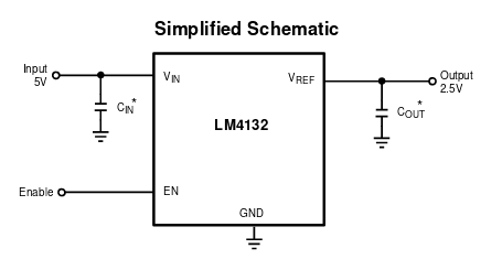
The datasheet gives a quite good example of how a symbol for this part can look like.
Screenshot%20from%202018-10-29%2019-45-18

Collecting the important information

To be able to create a symbol we need to find out what the interface of the part looks like. Meaning we need to know the functions assigned to each pin. This is found on page 3 of the datasheet.
In this case the part only comes in one package. If a part comes in multiple packages then we would need to decide for which package to make our symbol. (This will be handled in later tutorials)

From this we gather that there are at least 4 pins needed in the symbol. It makes sense to also include the non connected pin as it allows additional features to work. (One example would be the pin number filter of CvPcb)

Electrical type of symbol pins.

Detailed information about electrical types of pins can be found in the FAQ

We will assign power input to both the GND and Vin pins. (GND is shared for the input and output side. However power input should take precedence as it has stricter requirements.)
Vout will be of type “power output” and the enable pin of type “input”.
The NC pin wil get the pin type “Non connected”.

Lets get started

As a first step create a new project just for following this tutorial. Create a new symbol library within the project folder and add it to the project library table. A more detailed explanation of how to make a new symbol library is in a different FAQ article

Give the project the name “forum_tutorials” and place the library directly inside the project directory. Give the lib the name “tutorial_symbols” and add it to the project (also known as local) library table.

Symbol name

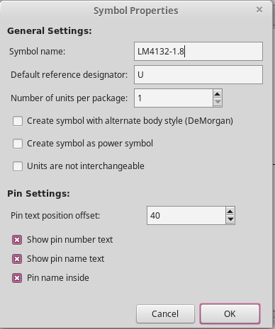
Give the symbol the name “LM4132-1.8” (We include the voltage as we will add other voltages as aliases later in this tutorial. You can include more parts of the part number if you want the symbol to be a bit more specific.)

The reference prefix

Choosing the correct reference designator prefix can be tricky. If you are part of an organization then check their guidelines. (There are many competing incompatible standards out there. Make sure what you make is aligned to what the reader of your schematic expects.)
If you are not then the wikipedia article about reference designators will be a good starting point. For this tutorial we use “U” as it is the suggested prefix for integrated circuits.

Creating the symbol

Right click on your target library (tutorial_symbols) and select “New symbol” in the context menu.

Fill out the opening dialog with the symbol name “LM4132-1.8” as explained above. Make sure the reference prefix is “U” (Should be the default).
Make sure that show pin numbers and names are selected as well as pin names inside. (This should be the default setting as well.)

Screenshot%20from%202018-10-29%2020-23-42

The result should look like this

The star next to the symbol name and library name means that there are changes to be saved. Use the save button in the File menu or the top toolbar to save your changes. The stars should vanish once you save.

Adding the pins

Choosing the correct grid for pin placement is important as mentioned in the introduction. For this tutorial we use 100mil grid for placing pins. Use view-> grid settings and select 100mil.

Lets start by adding the voltage input (Vin) pin. This can be done via the Pin entry in the Place menu, via the place pin button of the right toolbar or with the shortcut “p”. You will need to left-click if the pin settings dialog does not open. (Only the shortcut will open it automatically)

We set the pin name to “Vin”, the pin number to “4”, the electrical type to “power input” and the pin length to 100 mil. The position and direction values can be ignored for now as we will be able to move and rotate the pin around before we place it.
Press ok once you are happy with your settings.
Screenshot%20from%202018-10-29%2020-31-29

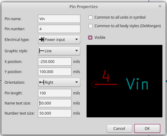
The pin will stay attached to your mouse pointer until you place it with another left-click. You can rotate it using the shortcut “r” as long as it is in this mode.
Notice that one end of the pin has a circle around it. This will be the point where you connect your wires in the schematic editor.
Place the pin somewhere on the left side of the origin with the circle pointing towards left. Don’t worry too much about the placement at this point in time. You can always move the pins around later on. (See the screenshot for inspiration. Left-click to place the pin.)

All future pin placements can be started with a simple left click. (As long as you are still in the “add pins” tool.) Next we add the GND pin which is also of type power input and has pin number 2. (Adding pins with similar setups is easier as kicad remembers all settings made in the previous pin placement.)
All other pins can be added in any order.

The only new thing is the non connected pin. This pins setings depend on your preference. I typically add such pins as invisible pins and place them inside the symbol outline to make it near impossible to accidentally connect them. You can leave them out completely or add them as visible pins. (If you add the pin then i would suggest to choose the electrical type “Not connected”.)

Finishing up the graphical look of the symbol

Reduce the grid spacing to 50 mil for everything except pins.

Add an outline to the symbol to make it obvious which pins belong to it. Such an outline is typically drawn in such a manner that the end of the pin (the one without circle) touches the outline and the other end points towards the outside.

For this simple symbol a rectangle as outline will be enough. Select the rectangle tool from the place menu or from the right toolbar. Left-click at your first corner. Move the mouse pointer to the other corner and confirm the rectangle with another left-click.
If you want to fill the rectangle then right-click on it. and choose edit rectangle properties (shortcut e). Select background fill. (Maybe also select foreground fill as an experiment to see what this option does.)

Move the reference and value field outside of the symbol even thought the visible fields will be automatically placed (can be deactivated) when placing the symbol inside the schematic. Doing this will make the symbol more readable in the symbol editor.

Moving any element is done by using the shortcut m while the mouse pointer is on top of it. Or by selecting move in the right-click context menu.

Adding additional information

This symbol would already be usable as is. Fill out the documentation fields and set the default footprint as well as the footprint filters to make it even more useful.
The user interface used in this part of the tutorial looks very different in the used version as compared to version stable 5.0.x and earlier. (Version 5.1 will look similar to this.)

All of this is done in the symbol properties dialog that can be reached from the edit menu -> properties or via the button in the top toolbar. (In version 5.0.x it is split into the field editor and symbol properties editor.)

Setting the footprint field

Setting the footprint field in the library eliminates one step when using the symbol. This does reduce the points where a user error can occur.

Left-click into the footprint field. A button will appear on the right of this input field. Clicking this button will open the footprint browser.

In the footprint browser select the SOT-23-5 footprint from the Package_TO-SOT library that is supplied with KiCad.

Setting the footprint filter

The footprint filter is used in the CvPcb tool as well in the add symbol dialog (if enabled) to reduce the number of suggested footprints.
We set this filter up such that it results in both the default footprint as well as its hand soldering alternative. (Ideally it should also future proof the symbol a bit)

Switch to the footprint filter tab of the dialog and enter *SOT-23-5* as the filter. The filter accepts two different wildcard characters. Star “*” stands for any number of arbitrary characters while the question mark “?” matches exactly one arbitrary character.

Adding documentation

Foul out the documentation field in such a way that it makes sense for you. The keyword field is used for in the symbol search features of kicad. For this tutorial we use voltage reference as tag.
Adding a valid link into the datasheet link allows easy access to the datasheet from within the schematic (right-click -> datasheet)

The newly added fields will be placed (by default) in the middle of the symbol. Move them outside to have a clean looking symbol. (Even if they are set to invisible, they are still shown inside the symbol editor)

Adding aliases for other output voltages

Adding aliases allows us to add different output voltage versions of this part without needing to maintain more than one symbol. Aliases are however quite restricted. Only a few fields can be specialized for every alias. One restriction is that all aliases share the footprint field and filters with their parent symbol.

Switch to the aliases tab to add and edit aliases. We add the alias for the 2.0V version of the part. Click the plus button and edit the alias name and documentation fields to fit your needs.

Adding user fields for better BOM output

Custom user fields allow for a more detailed BOM to be created.

Note however that all aliases share these fields. This means that we would need a separate symbol for every output voltage to be able to include full ordering information. For this copy the symbol inside the library instead of adding aliases. This of course increases the effort for maintaining your libraries.

As an example add a new field with name Manufacturer and value “Texas instruments”. Managing user fields is done in the General tab. Press the add field button and edit the field name and value accordingly.

The Result

Note that the alias is listed in the same manner as the symbol. However if you click onto the alias name, the symbol will be set as active. This can get quite confusing if the alias and symbol have very different names and there are other symbols in between them.

6 Likes

Creating a generic symbol for SE555

Disclaimer: This part assumes some basic knowledge explained in the previous section.

In this tutorial we will create a generic symbol compatible with a number of packages of the SE555 timer by TI.

This particular part comes in two types of packages. As 8 pin device in SOIC or DIP and as a 20 pin LCC. (See page 3 of the datasheet)
Notice that the pin number assignment between the 20 pin and 8 pin versions is incompatible. There is no way to model this nicely in kicad using one symbol. We therefore limit this tutorial to the 8 pin version.

The symbol name

A good name for this symbol would be SE555_8pin. (As with the previous symbol we leave everything else on default.)
new_symbol

Adding pins using the pin table

This part of the tutorial uses features introduced in version 5.1

Now to the fun part. Adding the pins. Lets try something different this time. We use the pin table editor to assign the correct pin names and electrical functions to the pins after we have placed 8 dummy pins.

Select the add pin tool and add a pin with pin number 1 and name it something obvious like DUMMY. (Makes it clear to you which pins still need editing in the next steps)
After placing the first pin press the Insert key on your keyboard. This will place another pin 100 mil below the last one. (It will automatically increase the pin number) Repeat this until you have 8 pins added.
pins_placed

Open the pin table editor (Edit -> pin table, or button in the top toolbar). It will look like this right now.

Change the pin names and electrical types to fit the component. After that it should like this.

Check the pins against the datasheet

To compare it with the datasheet you can sort it by pin name. (left-click onto the name header)

Finishing the symbol

The only thing left now is to rearrange the pins somewhat and draw an outline.
symbol_finished

You know the deal. Now it is time to add some information to the symbol. So lets fill out the datasheet link, description and keyword field for this symbol. Leave the footprint field empty as we create a generic symbol compatible to multiple different footprints.

Footprint filters

The symbol would now already be ready. Adding footprint filters will make using this symbol easier. The compatible parts come in 3 package types.

  • Part number suffix D is for a normal SOIC. The correct footprint in the library is SOIC-8_3.9x4.9mm_P1.27mm. A good footprint filter for this would be SOIC*3.9x4.9mm*P1.27mm*.
  • Part number suffix P is a DIP package with minimal lead spacing 7.62mm. The DIP-8_W7.62mm package would be a perfect fit for this. Set the footprint filter to DIP*W7.62mm*.
  • Part number suffix JG is also a DIP package. With slightly different measurements. (Ceramic instead of plastic package). It would definitely work with the above listed DIP footprint. It is still a good idea to add a specialized filter in case a better package is added later. I would suggest DIP*W7.37mm*.

1 Like

Multi unit symbol for the dual operation amplifier L272M

Disclaimer: This part assumes some previous knowledge that is explained in previous sections.

In this tutorial we design a multi unit symbol for the L272M op amp.

For multi unit symbols we have a choice to make. If we make all units equal (except pin numbers) then we can allow interchanging of units.
This would force us to include the power pins in every unit. Since version 5 ERC at least checks if such a duplicate pin is connected multiple times.
There are still some bugs that can arise when duplicating the pins. For this reason we will also create the alternative symbol with non interchangeable units where the power pins are placed in a separate unit.
Decide for your self which way you prefer. The official lib uses separate units for power pins except for symbols intended only for simulation.

Example with interchangeable units

Create a new symbol with name L272M_interchangeable. Set the unit count and the pin text position offset to 10. (The offset will make the symbol look nicer.) The rest can be kept as default.

Screenshot%20from%202018-10-31%2015-31-45

Symbol outline

Instead of drawing a triangle we copy it from another symbol. A good source is the generic opamp symbol found in the Device lib.
Use block select (press the left mouse button, drag the mouse, release left mouse button) for this operation. Select a block around the top left corner of the triangle and use crtl+c (or left click -> copy) to copy the triangle.

Paste the triangle back into our newly created symbol with the crtl+v shortcut (or right-click -> paste or paste button in top toolbar)
After placing it make sure that “common to all units” is selected. (or copy the triangle to the second unit as well.)

Adding signal pins

Make sure that synchronized pin edit mode is enabled as it will reduce the amount of work we have to do. This will add a copy of the pins on the second unit with an auto assigned pin number. This allows us to very efficiently create or edit such a symbol.
Screenshot%20from%202018-10-31%2015-36-57

Add the input pins to the first unit (pin numbers 7 and 8). For my triangle placement a pin length of 150mil allows the pins to be on 100 mil grid. (I choose this placement as this will allow the power pins to be added in a nice way.)
Screenshot%20from%202018-10-30%2022-50-22

For the output pin i did reduce the pin name size to 25 mil. (You can also leave the text size at default and use ~ as the pin name. Including a pin name will however make default net names more useful.)

If you now switch to the second unit you will notice that the pin numbers have a prefix -UB added. (Switching units is done with the drop down menu in the top toolbar)

We can now correct the auto generated pin numbers either directly in the canvas with the pin properties dialog of every pin (shortcut e or right-click -> edit). Or using the pin table as described in the previous tutorial.

Adding the power pins

The power pins will be added as duplicates to every unit. This means we select “common to all units” for them. A length of 175mil works quite well with the triangle placed like in the screenshots. I reduced the pin name size to 35mil. (Allows space between the V+ and GND texts)

Example with separate power unit

Modify an existing symbol

A very efficient way of getting to this symbol is to copy the generic opamp symbol from the Device lib. This is done by right-clicking onto the symbol name in the tree view and selecting copy from the context menu. Next right click onto our library name and select Paste symbol.

To rename the symbol edit the value field in the canvas. (shortcut e or right-click -> edit) In current nightly (or later in 5.1) this can also be done in the symbol properties dialog. As a name i would suggest L272M_separatedPower

Use the pin table editor as in the previous tutorial to fix the pin numbers. You can play around with improving the graphical style.

Splitting the power pins of an existing symbol into a separate unit

An alternative route would be to copy the symbol we just created (the one with the interchangeable units.)
Increase the unit count in the pin properties dialog (general tab) to two and select “all units are non interchangeable”.

In unit A disable “common to all units” for the triangle. Use the block copy trick to copy the triangle to unit B. (Any element for which you disable “common to all units” will be “removed” from all units except the one that is active while you deselect this option.)

In unit C disable “common to all units” for the two power pins. In addition delete the duplicated signal pins in unit C.

After this the 3 units should look like this.

4 Likes

Creating a custom power port (power symbol or power label)

Disclaimer: This part assumes a general understanding of the symbol editor. Basics are explained in the previous sections.

A detailed introduction to power ports can be found on stackexchange.
Short version of it: A power symbol is a special type of global label.

The label name is fixed in the symbol itself and can not be changed in eeschema. (It is controlled by the pin name) This is the main reason why you would want custom power symbols. Another reason might be that you are unhappy with the graphical style of the default symbols.

Symbol properties (new symbol dialog)

Use the intended label name (will become the net name) as the symbol name. This is for your convenience. Setting it to something else means you will not be able to know what the net name will become!

The Reference prefix must start with “#”. This tells kicad that this is a virtual component that should not get a footprint on the pcb. It also means this symbol is not included in the BOM.

Enable “Create symbol as a power symbol”. This tells kicad to include this symbol in the “place power port” dialog. This also has the side effect to do the same as starting the reference with “#”. (KiCad will kind of add “#” to your reference if this option is enabled. This behavior is however a bit buggy meaning it is still better to explicitly add “#” to the reference when creating the symbol.)

All other settings are made that way to make the symbol nicer inside the symbol editor.
Screenshot%20from%202018-10-31%2011-13-20

The pin (The thing that makes this part into a label)

Invisible power input pins are global labels. The label name is controlled by the pin name. Make sure the pin name and symbol name match! (This is for your own sanity. KiCad will happily accept a power port where this is not the case. Readers of your schematic will be confused if you do not ensure this rule is followed.)

Invisible power input pins can be used in other applications than power ports. (Some multi unit symbols in the official library still use this to connect them to power)
The power port is the only place where using this does not come with very strange side effects. (Do not use this feature for anything else than power ports unless you know what you are doing!)

You can set the pin length to anything. The power ports of the official lib use a length of 0. (Makes the symbol look nicer inside the editor)

Screenshot%20from%202018-10-31%2011-23-17

Finishing the symbol

Place the pin at the symbol origin. (This is just a convention making the symbol easier to use.) Make sure the graphic you create somehow shows where the connection point is. (Remember the pin is not visible in eeschema)

Move the fields around to make the symbol look nice and hide the reference field. (Does not really make sense to be shown.)

If everything went well then you should be able to add your symbol using the “add power port” button inside of eeschema

4 Likes