Approaching PCB track routing for a newbie

Can someone please point me towards a methodology to laying out a PCB. I have this circuit which doesn’t look that complex but my first attempt to route on a 2 layer board was pretty horrendous! Much more difficult than I anticipated.

Should I be using an auto-router ‘plugin’ or something similar?

There has been a couple of good threads before about this, some examples:

I still remember many years ago I read this document and used as base to start:

But in general it is the “craft” part of pcb design, it will develop the more you create layouts, find “inspiration” on what other have done, the constrains for the given board and your personal preferences.

The main issue I see with your layout are that the components seem to be placed pretty randomly. Placing the components at suitable positions should be something to really think through and will make drawing the tracks later much easier.

Then focus on the different types of tracks. High current lines should be short and thick. Data lines with nearby start and end should be routed together next to each other. And after that, any remaining lines can usually take more roundabout path’s unless they’re very high-speed or you need coupled pairs.

2 Likes

Adding a bit to what @Jonathan_Haas says, I would normally think about what constrains do I have on the board, which pieces you can move around and which ones need to be fixed at a given location.

For example, assuming that J5 is a connector for a Raspberry Pi, that makes its location on the top of your board kind of fixed (otherwise the board would just look funny), so I would keep that in mind when placing my components, are there any other component that needs to be fixed ? (is there and enclosure with pre-made holes?, maybe a daughter board on J4?, etc) If so, fix those components at their position.

I mostly would use a big grid (0.5mm or 1mm) to place big the components and if I have duplicated subsystems, like in your case, I would mostly focus on one, until I get a good layout and then just copy it into the other ones.

Think about where the signals are coming and where do they need to go, when selecting your final placing.

1 Like

Thanks! That gives me lot to consider.

But believe it or not I did give a reasonable amount of thought into the positioning of components. Obviously need more!

Yes positions of J1 and J2 are fixed, the depth and width of the board as well. J5, J4 and J3 can be moved around a bit.

Perhaps one mistake was routing it net by net, starting with Gnd, then the input supply rail. Just seemed logical to me. Should I start with signals and ‘work my way out’?

The other thing which I am embarrassed to admit is my lack of proper understanding of ground planes. Obviously I have none in my design at this point. But my prior thoughts were that ground planes were for boards with 4 or more layers and the ground plane would take up most of one of those layers, in which case a connection to ground only required a via through to that layer (thus eliminating the need for long and restrictive Gnd tracks and current induced noise). I know that is not quite how it works but is there an advantage of a 4 layer board to routing of Gnds? And is a 4 layer board worth considering for a circuit of this complexity (or should I say simplicity!). And similarly is it worth considering VCC planes or does that create one large capacitance across VCC → Gnd planes?!

Thanks for the great support BTW.

Positioning for me is the main work in designing PCB. If each element is where it is needed than routing is simple.

Till now all my PCBs are 2 layers and all of them have GND plane taking 100% of bottom layer. So except GND I design my PCBs as 1 layer. I use microcontrollers in QFP packages without thermal pad at bottom. This allows me to go with VCC under the microcontroller and go out through all corners and all VCC pins. That way GND and VCC don’t disturb my signal connections. At all digital lines I use serial 0603 resistors 47-100Ω. This makes switching current pulses lower and also helps if some tracks crosses. I prefer to use 0R then to make a hole in my GND plane. Free spaces at top I also fill with GND plane. All vias at my PCBs are GND.
Here is how it looks typically:

4 Likes

Advise I would offer is keep traces vertical on one layer, horizontal on the other as much as possible. This looks like a rather simple circuit, the more complex it is, the more you need to adhere to that strategy.
OtG

That was pretty standard advise some 20 years ago, but in the mean time signal flanks ave become much steeper, which create more EMI, and regulations for EMI control have been introduced, become mandatory (for everything being sold). Result is that for a good PCB design according to modern standards you at least need an (almost) uninterrupted GND plane on one side of the PCB. Very small interruptions of the GND plane, such as a “dog bone” track of 5mm long with via’s to jump over (or under) some other tracks is usually OK, but reducing such dog bones and keeping them short is one of the rules of thumb for PCB design.

PCB design is much more then replacing ratsnest lines with thin copper connections or letting an autorouter “do it’s thing”. The quality of the routing on a PCB can be the difference between a design working properly, and the same design not working at all!

1 Like

To underline a point above:

You may think that you are using a slowly clocked processor, or discrete logic gates that because you have a slow rate of data that EMI isn’t an issue. The problem with that thinking is EMI doesn’t come from steady state highs and lows, rather it is the transition between the two. Signal switching speeds are much faster now-a-days than it was 20 years ago, so old “works good enough” rules of thumb no longer apply. Sadly… (Darn physics always causing problems.) ;-D

Thanks Piotr
So rather than starting with the Gnd net and routing the track in a haphazard way to make all the necessary Gnd connections I would be better off:

  1. Creating a Gnd plane on the bottom layer
  2. Connecting all required Gnd connections using a Via through to the front layer and a short front layer track to the required device pad
  3. Then move onto creating Vcc connections using only copper on the top layer. This should be possible without having to use any vias through to the bottom layer (to be honest I find this hard to understand this as possible but maybe I will find it is possible once I practice - (late edit) Aha- the 0Ohm ‘bridge’ resistor makes this possible!).
  4. Then create other tracks on the top layer for all other interconnecting nets (again I find it hard to concieve how that is possible but maybe I will learn (late edit) again - the 0Ohm ‘bridge’ resistor makes this possible!)

Now I am studying your example some more. I gather this is the top layer only. I also gather that the track labelled ‘VC’ connects all the devices requiring VCC. I think I am starting to understand your use of 0R - you are saying that rather than diving down to the bottom layer with a via and then backup (which will create a small ‘hole’ in your ground plane) you use a 0ohm resistor on the top layer as a bridge OVER any tracks you need to avoid. That way the VC copper is extended to another island of copper. For example if the yellow mark below represented a 0ohm resistor.
image

1 Like

Paulvdh
The ‘dogbone’ in the bottom layer that you mention is what I gather Piotr avoids by using the 0ohm resistor on the top layer?

So perhaps this is over simplifying but would this be a reasonable summary of one way to go about it?

  1. Create a Gnd plane on the bottom layer
  2. Connect all required Gnd connections using a Via through to the front layer and a short front layer track to the required device pad.
  3. Create Vcc connections using only copper on the top layer (where possible) and 0Ohm resistors to jump copper tracks where necessary.
  4. Alternatively vias to short ‘dogbone’ shaped tracks on the bottom layer are acceptable but not optimal since they create a ‘hole’ in the otherwise continuous Gnd plane.
  5. Create other tracks on the top layer for all other interconnecting nets. Where other front layer tracks get in the way 0Ohm resistors or (with discression) the bottom layer ‘dogbone’ track can be used.
  6. Ultimately how often a bottom layer ‘dogbone’ or top layer 0ohm resistor is used is not that critical - but more a matter of personal preference.

There is not really a fixed order in which to route things, but before routing, footprint placement is an extremely important step.

Quite often, instead of using “zero ohm” resistors, you can also use real resistors that are already in your design to double up to jump over something else by moving them to the right position.

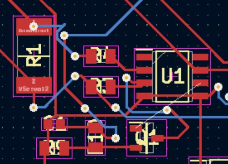
Routing the PCB is also an iterative process. For example from the lower right corner of your screenshot, you can easily get rid of two via’s by rerouting the blue part on the red layer as I did here in green:

image

And such things can be done quite often.
I also noticed that your tracks are quite thin. Probably the default, and that is a bit too thin to my liking, but to be sure, you first have to select a PCB manufacturer, and look at the design rules on their website, and make sure you setup coarser design rules in KiCad. Coarser design rules can often lead to a less expensive PCB. And design rules is not only track width and clearance, but also via drill sizes, annular ring sizes and some more.

Also, while routing, and you notice you have to go over/under another track, don’t regard that other track as an immovable obstacle. That other track can often be rerouted in some other way, so it does not form an obstruction anymore.

When you see a lot of layer changes in a small area:

image
Then often such area’s can be optimized a lot by re-routing the tracks, or by just rotating or moving a footprint.

Some people are annoyed that an “auto router” does not “automatically route” a whole PCB, and they are not finished yet after drawing a schematic, but making a good PCB layout is an art in itself, and it 's much more involved than just routing some wires. For example if you have a 10MOhm resistor, it can matter a lot if the “long track” is on the left or on the right pad of that resistor, and auto routers do not know such things. Placement of decoupling capacitors is also critical and there are many more factors to keep in mind during footprint placement and routing.

Reading about what things are important in a good design helps, but you also have to build experience by doing it. Treat it as a puzzle that is more fun then sudoku (I hate those useless games), but when you’ve routed a PCB nicely, you’ve got a real product that can be manufactured instead of a piece of paper full with scribbles that’s ripe for the garbage bin.

There are less 0Ω then you expect. At the fragment I showed there are only 2 of them. One jumps over 3 tracks (top-right from microcontroller) and second jumps over 2 tracks (bottom-right of microcontroller).

In my case it is mainly possible because at each digital line I use 47-100Ω as I have written.

No. It is 0603 ferrite bead. I power each digital chip through filter consisting of ferrite bead and capacitor. I use them ‘by definition’ to limit any disturbance propagating between ICs through VCC. They also (like these 47-100R) help with PCB routing. In many cases i don’t need to add any 0R while routing my PCBs. At this whole PCB I used only 3 0Rs to cross wires. There are also 3 others but they are used to configure PCB for two power modes (48V PoE and 12V).

You need not to follow my way but adding 3 0Rs to BOM costs zero, zero, nothing. In no other PCB I had to use as lot as 3 0Rs. Typically I need 0 or 1 of them.

Search at my PCB tracks which are not tracks - they connect nothing :slight_smile:

As others have mentioned, placement is quite important so if we work with the assumption that the connectors are fixed

  1. rotate U3 90deg counter-clockwise - easier fanout to J1 and J2
  2. rotate R1 180 deg and move between J1 and the left-hand connector
  3. you have at least two instances of “via in pad” (R1, J4), you really don’t want that at this stage

there are plenty of other suggestions that are viable but 1st things 1st

1 Like

I intend to start again with the routing and yes I will give the placement and orientations more thought.

But after that would defining the Gnd plane on the bottom layer and then connecting all my Gnds using vias to that Gnd plane be a logical first step? After Piotr explained his layout that seemed to be an obvious and much better way of approaching the Gnd connections thus dealing with a large portion of the job.

Furthermore let’s say the Gnd plane has been defined. Should there be a need to route a small track segment through that Gnd plane does Kicad somehow have the ability to create the necessary hole in the Gnd plane to make room for the non-Gnd track?

If you dedicate a full layer to the GND net, then it does not matter much if you route that at the beginning, or near the end, because it’s always easy to route to.

All internal geometry for copper zones is calculated semi-automatically when you depress the b shorcut key. I usually draw something like a pentagon around the PCB, because the zone geometry calculation also keeps it’s distance from the edge of the PCB. This last is a setting in: PCB Editor / File / Board Setup / Design Rules / Copper / Copper to Edge clearance. Drawing an (irregular) pentagon around the PCB PCB has the advantage that if there is something wrong with the PCB outline (on the Edge.Cuts layer), then this becomes obvious immediately, because the whole pentagon gets filled with copper.

I left it for the end of work. If you can connect to GND really everywhere why to lock footprint positions before routing signal tracks.
So my first step was always to hide GND net to see only connections I have to do. I also changed VCC and other power connection lines to be red (just to know which connections need be wider).
Then I did placement thinking of each connection which way I will route it. To help see what are my plans I sometimes did a temporary tracks just to make connection lines be moved to place showing how I plan to route it.
When I moved to KiCad I couldn’t hide GND net. My way around was to place GND plane on top and frequently use ‘b’ hotkey. That connected GND to element pads hiding the GND net lines.
In V6 you can hide GND connection lines, but I did not use V6 yet.

If you route other net at bottom then KiCad will calculate the GND zone for you (hotkey ‘b’). Just make some experiments.