Solved - First PCB Looking Good, I Think

If you have the time and are interested please look over the layout and provide constructive advise.
I’ve already received some very good advice when struggling with learning KiCad Pcbnew to resolve issues and the learning curve.

This is a fairly simple design and runs at no more than 200 KHz clock rate. The three devices missing on the 3d View are modules with decoupling caps and such built in. So there is no need to have any on the PCB, I think. The U1 chip is a level converter, 3.3V to 5V. One U1 output switches at 100 KHz and the other two rarely and at different times. One load per output. Should I put a decoupling cap?

I noticed the three right side connectors Pins 1 are not all on the same side. I’ll fix this. And the pin headers can be closer to increase area for future shields that stack on top of this one. But I think the DRC failed when closer. Issue to resolve when moving them closer.

I’m heading out for the day. Hiking in a remote local.

HI,

I only design boards for myself. So I don’t have the “eye” some of the other folks have.

The first thoughts that hit me are:

  1. J1 has some funky green traces I don’t recognize. Perhaps they are wayward traces that become part of the ground plane.

  2. You could increase your clearances with a little fine tuning i.e. U3 Pin 11 and the via near SW1, P1 Pins 1,2,3 etc.

  3. Perhaps a pet peeve of mine is the inclination to go to the minimum requires spacing, via sizes and trace width.

    • Vias are electroless plated. They are nowhere near the quality of the traces. Google “pc board via cross sections” and you will see how bad they can be. I always double (or close) the via diameter. In most locations it makes no difference in the layout but they are much more robust. On heavy traces I’ve use up to 4 via’s on the same “stitch through” locations. No cost and 4X the capability.

    • Trace width and spacing. Yes the board mfg can make them but with a hobby board if you ever need to cut and jumper a trace it becomes very difficult to do so on a thin trace packed between two other thin traces.

U2: Pin numbering looks wrong. you can eliminate a via at pin 10. I’ll assume what ever goes here will clear the resistors?

R4 & R6: you cut the ground plane needlessly (admittedly a small effect)

Good luck

John

1 Like

Very helpful, Thanks

U2 does have odd numbering, the way the module is numbered unfortunately. It does clear the resistors. I changed several ground plain connections for ease of soldering or increased the connection due to higher peak expected currents.

Multiple vias in power connections is a good idea. Improving clearances done, didn’t see that.

What manufacturer do you use for you PCBs?

After looking over your comments and fixing them I started noticing similar etches too close to pads among other better track routes.

@JohnRob Who manufactures your PCBs?

After looking over your comments and fixing them I started noticing similar etches too close to pads among other better track routes.

That’s good. For hobby circuits you want as much space as you can and widest traces you can (within reason.

To help prevent errors, before ordering your boards, print them out at 1:1 and lay as many parts on it as you can (one at a time is OK) just to be sure your footprints are correct. One issue that is common is a part layed out upside down. Relays are most common mistake.

I’m usually not in a hurry so I’ve been going to JLCPCB. Else I would go to https://oshpark.com/

1 Like

I can not do a decent board review from a few screenshots.
Even though you say your modules have built-in decoupling capacitors, I would still add more decoupling capacitors. Especially with high current devices such as motor drivers.

The decoupling capacitors are not only used to smooth the power supply to IC’s, they are also for smoothing the electrical noise that IC’s generate when switching and preventing it from reaching other circuitry.

What is the current capacity of your motors? It’s probably not strictly needed, but I would still add an extra via in the high current motor tracks (and power supply tracks). Via’s are cheap, you also have plenty of room. Have you used the PCB calculator (or a table) to make sure your track widht is adequate for your motor drivers?

Motor drivers (and any high current switchers) also do not only need decoupling capacitors, they also need buffer capacitors. These are usually bigger, but cheaper electrolytics in the range of 100uF to 1000uF (or even bigger especially for big motors). 2 electrolytics of 220uF each are usually better than one big capacitor of 470uF. But to be sure you have to check the ESR value from the datasheet.

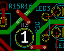
In this area your GND plane is very narrow. If it is a spot which has high motor currents, then make it wider.
image
You should be aware of how the currents flow through the GND plane. Print out the PCB bottom on a piece of paper (preferably enlarged scale) and draw the main current paths through the GND plane on the paper.

Keep as much of the tracks on the top of the PCB, and make cuts in the GND plane as small as possible. This reduces emitted EMI noise, and also lowers voltage differences over the GND plane.

Why do you have 4 SMD resistors and 16 THT resistors?
The THT resistor also look smaller then the “most common” size. Are you sure they are the right size?

If this is to fit on an “arduino” board with a big square USB-B connector, then you have very little clearance between the top of the connector and the bottom of the PCB. There is no room left for pins of IC’s and connectors sticking out in that area. If you can not move the connectors, then cut of the pins before you put those components in the PCB. Make them so short that they do not stick out of the PCB.
Also put a few layers of insulation tape, plastic foil or cardboard between the metal USB connector and your PCB to prevent any possibility for shorts.

Where does power for the “arduino” board come from?
How is power routed?
What happens if the “arduino” has power, but this PCB does not (or vise versa).
You should not apply logic signals to IC’s that do not have a working power supply.

Apart from these remarks. Your board looks a lot better than I’m expecting for a first design. You have for example even thought about lowering GND plane impedance by making some bridges over high current tracks:
image
But why not simply move those tracks to the top layer, and have a continuous GND plane?

2 Likes

@paulvdh First thanks for taking the time. If you think it would help I’d share the kicad pcbnew after working it over. Would that even be possible without libraries? Does Pcbnew pull in all the information required and not continuously reference libraries?

I was concentrating so much on the layout I forgot to consider the board to board height restrictions. Hmmm… I look into that before proceeding. I can remove the Arduino power connector and go with the Arduino Leonardo. Or move things out of the area.

The Arduino power is from the P1 the +10V, OMG… P1 pin one is on the left and my schematics have it on the right! Thanks for the Vin question!

Given @JohnRob 's feedback I already increased the vias in the motor driver tracks and other power tracks that traverse layers. The peek current is defined by the two surface mount resistors next to U3 & U4. These resistors see a peek of 200 ma. Peak driver current is as high as 4 AMPS. But it is a switch none the less, DRV8833. Rise/ fall time ~200ns. The motors have low resistance and roughly 50uh, slows the inrush current somewhat. I add caps to the motors to reduce high frequency noise. Maybe there should also be across the connector as well? Or would that set up some kind of current loop in the wiring. Another point I use the drivers in soft break mode. This means when the driver is disabled the current is allowed to flow from motor back to motor. No quick reversal of motor direction.

So peak current to each driver module is 4 amps as well. I am not sure at al about proper power etch widths. I did use a calculator it appears ok. But experience trumps all.

I’ll work on the ground plane overall and near the motor drivers. Easy to fix that area.

The SMD resistors are current sensing. The values range from 0.0? to 0.2 ohms depending on desired maximum current. The others are for ease of hand soldering and assembly.

THT resistors are 1/8 Watt and I’ll double check with printing out 1-1 and use the parts. I did look them up and measure so I’m pretty certain.

Power routing… U1 requires +5V on pin 14 from P1 +5 V (Arduino supplied). It is a level 3.3V to 5V shifting tri-state device always enabled.

U3&4 are Pololu DRV8833 motor driver modules and gets power from top right connector, 4-10 volt adjustable range.

The Arduino power comes from this module via top left connector 10V input. Arduino’s +5 V goes to the level shifter U1 and +3.3V to U2 FPGA module. So the Arduino sees no signals until it is powered up. From the DrV8833 spec… “There is no specific sequence for powering up the DRV8833.The presence of digital input signals is acceptable before VM is applied.” The one DRV8833 logic output is oc and is pulled up by a resistor tied to +3.3V.

Thank you for all this feedback… combined I just may end up with a PCB that works and is reliable.

I look forward to more feedback regarding track widths, capacitors, and that not yet realized. It’s been over 30 years since working at this level. This is fun! Was into ASIC logic design.

Pcbnew has copies of the library symbols embedded in the pcb file itself. You can easily check that by for example unlocking the pad locations relative to the part and then move a pad. This would not be possible with the default libraries, because the are (or should be) read-only. You can also directly load a part from Pcbnew into the Footprint editor by hovering over it and pressing [Ctrl + e], and when finished, put the new part back on the PCB again.

Eeschema is dependent on the project_cache.lib file.
This is a cumbersome hack, and will change with KiCad V6.

If you want to share the project, the easiest is to zip the whole project folder (inclusive the folder itself), and remove redundant files such as the backups of the schematic and PCB.

When your project is finished, and you want to archive it, always add a .pdf version of the schematic. This makes it easy to share your work or to view it yourself on another PC where KiCad is not installed. It has also saved me some times when the schematic got damaged because of updating from old versions of KiCad in the wrong way a few times.

Also, if you put the .pdf files on gitlab or similar, they are much easier to view and get a quick overview than by first cloning the whole project and then opening it. The .pdf and the .svg variants can be viewed almost anywhere.

2 Likes

Trace width is also not an exact science.
Making traces wider lowers the resistance and this lowers the temperature (resistive heating) and voltage drop. (V = I * R).
If peak current happens during short times, then the RMS current may be more appropriate for calculations.

1 Like

@paulvdh, @JohnRob

I’ve taken in all your valuable feedback and did a bit of work to improve the layout. Much improved.
Thanks

1 Like

Looks good.
Every remarks left will get smaller and smaller.
But still, no detailed review without complete board.
(I am also not in the mood for an extensive board review at the moment anyway).

I’m also still missing big buffer caps for the motor drivers.
The screenshot below is known as “CNC shield”

1 Like

This topic was automatically closed 90 days after the last reply. New replies are no longer allowed.