KiCad has the ability to create custom design rules for DRC that modify how clearances are calculated and applied.
The formal documenation for these custom design rules is on:
This FAQ article is an attempt / start to collect examples of such rules.
A short description on what the goal of the rule is, preferably with a link to a picture already on this forum (just copy a link from the original and post it here. No need to copy the whole picture. This forum software understands).
The actual text of the rule itself.
A direct link to the thread the rule was posted.
More? (I’m no expert on these rules myself).
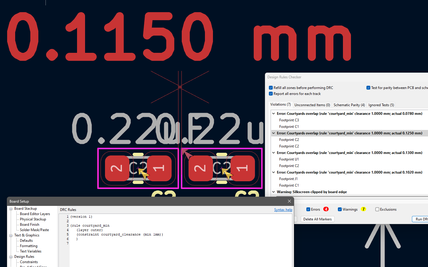
There are also examples of rules in: PCB Editor / File / Board Setup / Design Rules / Custom Rules / Syntax help which is the small inconspicuous light blue text in the upper right corner:
Creating a big clearance between net classes in a “High voltage” section and the rest of the PCB
The trick here is to create netclass names starting with a recognizable string (“HV”) and using that in the rules.
Rules are also applied in order, and the thread discusses some of the consequences of that.
(version 1)

(rule "LoW cLeArAnce BeTWeen neTS of THe SAme HV potential"
	(constraint clearance (min 0.2mm))
	(condition " A.NetClass == B.NetClass && A.NetClass == 'HV*' " ))

(rule "HIgH cLeArAnce BeTWeen neTS of dIfferenT HV potentials"
	(constraint clearance (min 5.0mm))
	(condition " A.NetClass != B.NetClass && A.NetClass == 'HV*'  && A.NetClass == 'HV*' " ))

(rule "HIgH cLeArAnce BeTWeen LV And HV neTS"
	(constraint clearance (min 5.0mm))
	(condition " A.NetClass == 'HV*' && B.NetClass != 'HV*'" ))

(rule "Reduced cLeArAnce for HV PoTenTIALS cLoSe To comPonenTS"
	(constraint clearance (min 1mm))
	(condition " A.insideCourtyard('*') && A.NetClass == 'HV*' "))
Although personally I would just draw a copper track (with a certain width) through the zone to ensure a certain width as I also mentioned in that thread. But to each his own solution.
Tracks are often narrower then pads, and this limits the maximum clearance that can be used for tracks, while wider clearances for tracks are often preferred to reduce capacitive coupling between adjacent tracks. Especially for fine pitch footprints it is nice to fine tune this.
This can also help if you prefer to use a combination of track width + clearance that fits on your grid.
These rules work on themselves. It was just a test, using wildcard in the footprint names is probably better in a real project. Unfortunately this had serious consequences for the interactive router. It blocked most of it’s functions and also created DRC violations. I opened an issue for this on gitlab and the issue was picked up by James J · GitLab and fixed in less then an hour. As a result, this will probably be included in the next bug fix release of KiCad V8.0.5 in a few weeks.
insideCourtyard() is deprecated, use intersectsCourtyard() instead.