Because this topic raises problems and questions perennially, here is another explanation which goes into more details. KiCad version 5.99 (pre-6.0, which is essentially similar to at least up to version 9) is used for reference.
In KiCad changes made in the schematic must be propagated to the layout explicitly with Tools → Update PCB from Schematic. Notably KiCad must have some way to keep the connections between symbols and the corresponding footprints. Normally it’s done using internal unique IDs. Each symbol in the schematic has an ID. This is from a .kicad_sch file (KiCad version 5.99):
(symbol_instances
    (path "/800ee8b3-48b2-4453-9721-def5d406289a"
      (reference "R1") (unit 1) (value "R") (footprint "Resistor_SMD:R_0603_1608Metric")
    )
  )
The unique ID which is path in the file, here path "/800ee8b3-48b2-4453-9721-def5d406289a", actually has the hierarchical sheet path and the ID of the schematic symbol. From now on we’ll use just “ID” for short. When the schematic and the layout are in sync the .kicad_pcb file has the corresponding footprint:
  (footprint "Resistor_SMD:R_0603_1608Metric" (layer "F.Cu")
    (tedit 5F68FEEE) (tstamp f4991ce1-17e3-423c-82e2-b0c4e9847e87)
    (at 155.1 98.7 90)
    (descr "")
    (tags "resistor")
    (property "Sheetfile" "test.kicad_sch")
    (property "Sheetname" "")
    (path "/800ee8b3-48b2-4453-9721-def5d406289a")
    (attr smd)
    (fp_text reference "R1" (at 0 -1.43 90) (layer "F.SilkS")
The same ID is there and it’s the internal link between the symbol and the footprint. Also the reference designator is in sync. The new footprint has been created in the layout with the normal procedure:
- Add symbol to schematic.
- Assign a footprint to the symbol if the symbol doesn’t have it already.
- Annotate.
- Tools → Update PCB from Schematic (with the default linking option – in 5.99 like this):
This workflow has added the symbol’s footprint into the layout, added the symbol’s ID to the footprint and updated the reference designator.
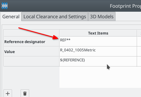
Compare this with the situation when we add a footprint directly to the board with Place → Add Footprint:
  (footprint "Resistor_SMD:R_0402_1005Metric" (layer "F.Cu")
    (tedit 5F68FEEE) (tstamp 20286e5f-01fb-414f-8f46-8a8e2dee937d)
    (at 152.209 95.108)
    (descr "")
    (tags "resistor")
    (attr smd)
    (fp_text reference "REF**" (at 0 -1.17) (layer "F.SilkS")
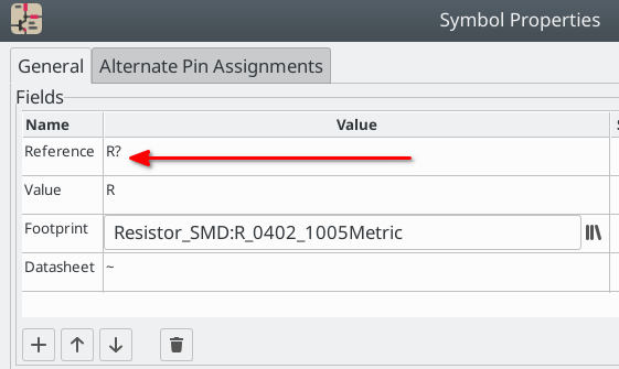
There’s no symbol’s ID (path) there, and no meaningful reference designator. Even if you add a new symbol to the schematic and assign footprint “Resistor_SMD:R_0402_1005Metric” for it, there’s no connection between the footprint in the layout and the symbol in the schematic even though the symbol has an ID.
The user can’t edit the ID through the KiCad UI, but the reference designators can be changed.
If both are changed to, say, R3, we have a symbol and a footprint with the Reference R3, but still the footprint and the symbol aren’t linked internally.
So, what we must do is to use the second linking option in the Update PCB dialog. We match by reference designator. Now KiCad finds the symbol R3 and the footprint R3. The footprint’s symbol ID is changed to the symbol’s ID. And now the schematic and the PCB are totally in sync again. After that the default linking method by the ID can be used again.
When to use each option?
The most common workflow is adding symbols to schematic, annotating them and then updating the PCB. The default match method by ID should be used for that. Also after partial or full re-annotation of the schematic the same option must be used. In these cases KiCad adds the ID to new footprints and finds the old footprints by the ID.
The other option – in version 5.99 “Re-link footprints to schematic symbols based on their reference designators” – should be used if for some reason the connection between the symbol and the footprint hasn’t been established with the normal workflow first or it has been broken. But in this case there must be matching reference designators. Otherwise there’s no way to tell which footprint belongs to which symbol. The use cases may be for example
- footprint has been added to the layout first
- a symbol was deleted and then re-added (a new ID was created for the new symbol)
- part of the schematic has been moved, i.e. cut and pasted, between hierarchical sheets (even with Paste Special keeping reference designators)
- part of the schematic has been cut and pasted even within the same sheet (pasting doesn’t keep the ID)
- the whole design was made with separated schematic and layout, for example following manually an example board
- or the schematic and the layout were created with an importer script which can’t add the IDs.
Avoiding problems
The two matching methods can’t be used at the same time. Therefore the edits to the schematic/PCB should also be limited so that you either add symbols with footprint associations normally to the schematic and update the PCB by the default method, or you add non-matching footprints and symbols and then update using the “re-link using reference” method. If you try to mix the two methods you may run into situation which needs fixing or causes confusion.
In general, it’s better to keep the changes simple and clear. Do one kind of thing at a time and update the PCB. Then do the other thing. Don’t mix different kinds of changes.
If you want to update or change a symbol but keep the footprint, don’t delete and re-add the symbol. Instead, use Change Symbol or Update Symbol. Those functions keep the ID while deleting and re-adding changes it.
Version 5.99 has the new backannotation feature, “Update Schematic from PCB”. It’s possible to make certain changes in the layout and transfer them to the schematic. “Geographical annotation” is one nice application for that. If you use backannotation – are planning to make changes which need backannotation – make sure the schematic and the layout are fully synced first using Update PCB from Schematic.


