Seek review my first PCB design

Hello –

Please find linked compressed project folder, contents of which I seek review and feedback. Much appreciated.

LoPower2.zip

The design is an environmental sensor, just temp and light, baro and humidity. Laid out on proto board about four years ago, near continuous service over that time. Had to clean a spider nest from one so decided to take plunge and design a pcb. Sensor data is broadcast to receiver and logged to SD card, basically.

Thank you in advance,
Mark

First the schematic. I opened it in KiCad V5.0.2 and the symbol for yu uC had to be “Resqued” because you are using old symbols. Are you still using KiCad V4, or have you KiCad V5 mixed up with KiCad libraries from V4 (this happens quite often)?

Then, the overal view of the schematic is quite good, a few small points:
You’ve used the “Earth” symbol instead of the “GND” symbol for GND. These have different meanings and purposes, but for the design of the PCB itself it does not matter, the’re just connected together.
You’ve also used global labels for Vcc. Using the VCC power symbol for Vcc makes your schematic a bit more readable.
You’e used global labels for everything, (I do that too sometimes), for your nex project try to get acquainted with the local and hierarchical labels. The “Getting started with KiCad” manual is a bit out of date, but the reference manuals for the KiCad programs are more up to date, and you probably learn some tricks when reading them.
http://docs.kicad.org/

Then I ran an ERC check, and it gave an error on AVcc.
AVCC of AVR controllers are a real power input, and they need to be connected to VCC. It’s common to add a capacitor to Aref, but not mandatory. If you place it on the schematic (+ PCB) you can always decide later if you want to add it.
I was missing a GND pin. But that’s KiCad’s fault. I find it personally a bit annoying that “Agnd” (Pin 22) is implitly hidden in the schematic. This is a known “fault” though and likely to be handled differently (hopefully better) in KiCad V6.

On any uC board I like to see some choke or inductor on the power supply inputs. This makes almost every uC board more reliable.

Looking at the PCB now. Double sided PCB’s are cheap now, and this is clearly meant to be made by a manufacturer. Youve put quite some effort in a neat layout, putting all the text on the silk screen right etc.

I first ran a DRC:

Pcbnew / Inspect / Design Rules Checker.
If found 2 errors: “Track near Via” near C3 and an “Unconnected pin” which turns out to be a small floating dot of copper under “R4” Silkscreen text.
You should always make sure you have no DRC errors left before having a board manufactured. I moved the via a bit, and then did:
Pcbnew / Edit / Cleanup tracks and via’s.
After this I re-run DRC and there were no more errors (But you still have to change AVCC).

Apart from your AVCC pin it looks like this board will work.
The next biggest thing is the total abence of a GND plane.
I first removed the whole “Earth” net, and then used:

Pcbnew / Place / Zone

to draw a pentagon around your board, connected to the “Earth” net.
After that I clicked on the edge of the zone and pressed “e” to edit it and changed the “Clearance” and the “anti pad clearance” from 0.508 mm to 0.3mm. This makes the zone sneak through all the 0.1" spaced pins and makes a nice solid ground connection.
The board now looks like:


I drew a pentagon around the board for the Zone boundary, because KiCad should keep the zone nicely within your board outline.
If it does not and the whole pentagon gets filled, you see it immediately in Pcbnew, or in a Gerber viewer.

The zone is not finished though. Ideally you have a power connector, then a filter on the input power, (Choke + caps), then the voltage regulator, and only then the connection tho the GND (Sorry, “Earth”) net.
When working with GND planes there are a few more wize rules:

  • Make them as continuous as possible, no big cutouts for traces.
  • Be carefull with mounting holes.
    Sometimes you want to keep the GND zone away from mounting holes.
    Sometimes you want to connect the GND zone to the mounting holes.
    KiCad has some nice mounting holes with included annular ring, with the size of the screws for the mounting holes.

On the schematic I did not notice the reset circuit. It is a bit clearer if you put the reset switch, C6 and R2 close toether on the schematic. Ceramic capacitors (C6) can deliver high peak currents. This puts a lot of war on the switch (it may deliver 10A peak currents, the switch is not made for that) and such high current peaks put a lot of noise in the GND plane (Although both are not very important for the Reset switch).

Finally some small notes:
You put your resistors vertically on the PCB. This way they easily get bent, or misaligned. It “looks better” if you lay the resistors flat on the PCB. With analog circuits this is often also very handy because you can route a number of traces under the resistors.

If you work with a coarse grid during the component placement, the board also loos neater. A coarse grid also makes it very easy to fix the locations for your mounting holes and board outline.

Currently I measure approx 1.56" * 2.21", or 39.62mm * 56.13mm for the outline. I do not know if this on purpose (I did notice the edges are perfectly square to each other), or accidentally, but with the use of a coarse grid it’s easy to make nice round numbers.

LM35 is a relatively expensive temperature sensor (EUR 5). Compare that with for example the MCP9700 ( 23ct).

C1 is most likely the highes part on the PCB. If you make a bit of room around it, you can bend it over and lay it flat on the PCB. (Possibly with some glue).

Keep a bit of area clear around the reset switch, so you do not touch other components (C6, R2) when you try to push the reset switch.

Everything on this board is relatively low power, but still I like to see some fatter traces for the Vcc net. This will also give you some practice for working with different trace widths.
You can do this with:
1). Pcbnew / Setup / Design Rules / [Add]
2). Add a name, for example “Thick” & OK.
3). Change track width and clearances, and via settings.
4). Select your “Thick” net class in the right dropdown box.
5). Move all the “power” nets to the right with the [ >>> ] button.

You should also change the “Via Drill” and “Via Dia” of the default net.
0.4mm drills are very thin and break easily, and are therefore more expensive to manufacture. Drills of 0.6mm or thicker are generally OK.

This is what I made of it, (but sizes ar a bit arbitrary).

If you now run the DRC again, there should be errors, but there are not.
Apparently the design rules for the widht of the tracks are not checked in the DRC.
You can update the track widths of existing tracks with:

Pcbnew / Edit / Edit all Tracks and Vias / Global Edition Option: / (*) Set all tracks and vias to their Netclass value / [ OK ]
Now you can see that the thickness of the tracks of several nets have been updated where possible, and keep a small thin section if the thick line does not fit (For example Vcc net between pins 3 and 4 of the AVR.)


You can easily clean them up by drawing a new line around the AVR pins.

Silk screen text placed over Via’s gets easily distorted. I recommend either moving the via or the text.
image

And finally, never forget to admire your own craftsmanship :slight_smile:


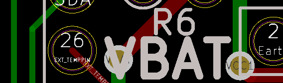
Look at your PCB from all sides. You often spot small (or big) things that can be improved. Do you see how close R2 is to the (footprint of the missing) Reset switch? The hole in the VBAT silk screen text?

And finally: always do a last DRC check before making Gerbers, and afterwards have a look at the Gerber files for obvious mistakes.

Even mor final remarks:
Your IMG_7395.JPG is quite dusty.
You can safely delete the backup files (LoPower2.bak, LoPower2.kicad_pcb-bak) and the netlist (LoPower2.net) from zip archives.

4 Likes

Thank you sir for your detailed response in re the schematic.

I’ve been tinkering a bit with your project. :slight_smile:
I hope you don’t mind.

What I did in short:

  • Schematic: Added Vcc to pin 20 and added cap for Aref.
  • Schematic: Added mounting holes.
  • Exchanged mounting holes for holes with rings, so the scews dont touch GND.
  • Rotated PCB 90 deg. so if fits better on my monitor.
  • Added GND plane.
  • Fattened up traces (Most from 0.25mm to 0.35mm).
  • Optimized GND plane by making cutouts smaller.
  • Rotated U3 180 deg. becausee of routing.
  • Fat outline, to increase the claring of the GND plane to the Edge.Cuts.
  • Moved some of the texts a bit.
  • Added full ISO8601 date to your revision.
  • Added KiCad logo on the backside (It’s i the library).
  • Added 3D symbols for a (smd) switch (closest from the lib) and for U2.

2019-03-03_LoPower2.zip (51.9 KB)

Someother things I noticed:

  • there is a dot near pins 1 of some connectors, but on ICSP it’s in a weird location.

Some things I woud do if it was my own project:

  • Remove the 3 leds + resistors and put a prototyping area there.
  • Bigger pitch for power (Bat) connector 5.08mm for screw connector for example.
  • Move the AVR a bit up and relocate (or remove) light sensor to make proto area bigger.
  • Put a Choke / filtering in power connector.

Yes, yes, thank you kindly!

Several of the small things I resolved: the dot of track, tying AVCC to VCC, &c.

After posting I was looking into details of a ground plane, “copper pour”, still a bit confused on difference. There is a 2.4GHz radio in there so was wanting to understand how to enhance its performance. I hit “highlight net” on the GND/“Earth” and was looking at what I was working with. But, yeah, I had no idea how to create the groundplane, and your tips will get me quite far along the way.

In re RESET switch. Correct, I need more room for my fat finger. In the circuit, R2 holds reset high, C6 comes over from DTR (reset) on the FTDI, as oft mentioned in articles regarding building these AVRs up the “Arduino” way. Yes, that’s my level of competence, ya know as a hobbyist. Hehe.

Yes…there is an nRF24 radio atop the 2x4 headers, so height on Z adds up. I attempted to place the passives central to board, guard with the male headers. I try lay them down and see what can make of that.

Hahaha…I was swapping grid dot density so often I got lost. Edge Cuts is just where I could get modest clearance to components on board and was kinda arbitrary. It does fit within footprint of 3xAA batt holder.

Thank you for the tips on track widths. I used the default width just to get started. All the tracks were laid by hand/eye/trial and error. There was not an apparent auto-route feature that I could see, one that can just click a button and watch KiCAD run trace possibilities. I think I got more good from doing it the slow way.

Wait, wait…oh, my friend…

Yes, I was thinking of getting rid of the LEDs and adding in a kludge area. The LDR can come off as it will probably be wired external, just the LM35 on board measuring internal to housing (sitting outside in sun). Batt will just be solder leads from below.

The big one though is placing “choke/filter” on power. Sorry, I am fairly lacking a well-rounded knowledge of these things. I look it up though.

Mahalo nui aloha e,
Mark

Out of curiosity, for what reason did you add an exclusion zone for this plane around the power supply connector and the regulation circuitry ?

The Idea is to do some filtering on the power input section before a connection to the GND plane is made, to keep the GND plane clean from noise picked up by the power input antenna.

To be effective this begs for some chokes, common mode filter, or even a SMPS voltage regulator, but I did not want to modify Bambuino’s design too much, nor did I want to put too much time in it.

C2 and C3 are were placed by Bambuino, and the input power goes through these capacitors before it reaches the GND plane. Hopefully these will attenuate noise. For the same reason I’ve also explicitly routed the input power from the connector to the first capacitor, and from the capacitor to the voltage regulator. The effect will probably be minimal, but a bit is better than nothing.

I have a bunch of uC’s on a self designed home automation project,(Power via long CAT5 cables) and I’ve concluded that no uC circuit can work reliably without some filtering on the power cables (and other long attached wires). uC’s tend to get upset easily by nearby switching of low voltage halogen lights with real transformers, or fluorescent lights with inductors as ballast.

A Ferrite bead or choke is a component that has very low DC resistance (So it lets your power through), but at higher frequencies it acts as a resistor, and combined with capacitors it filters out short, high frequency, glitches.
https://en.wikipedia.org/wiki/Ferrite_bead

Reviewing the data sheet and some app notes, AN2519, &c., the only inductor called for is 10uH tying AVcc to Vcc. In past, I never incorporated because of lack of knowledge and the myriad choices of components from a vendor…RF choke, EMI suppression, Power filtering? Bourns 78F series? Laird 28L’s? Although, app note AVR040, fig 4-3, there is illustrated an LC circuit, but nothing there specific enough to be of assistance to me.

So, back to the books, and reviewing this thread. I’ll get it, I’ll get it.

Thanks folks!

As an aside, I tried Eagle and Fritzing years back, and dropped it because of steep learning curve. For some reason KiCAD took to me with my first try. Probably more credit due the developers than to myself. Hehe.

@paulvdh, I am wondering what you did to make kicad display the 3D view? My pcbnew (version: 5.0.1+dfsg1-2~bpo9+1) only shows the PCB with silkscreen and plated through-holes when I bring up the 3D-Viewer–no components, just an unpopulated PCB. Same for your 3-3-19 revised version. Do you remember what you did to make the components show up in the 3D -Viewer as your photo shows?

I run Linux here, and with Linux the installation of KiCad consists of several parts.
The Library with 3D Symbols is not installed by default

What I did was:

sudo apt install kicad-packages3d

There is a bit more of that in:
https://forum.kicad.info/t/problem-with-ppa-install-kicad-v5-0-2/15437
You may also find some hints in the Download section on the KiCad site for your particular OS:
http://www.kicad.org/download/

1 Like

@paulvdh, That worked splendidly !! thanks so much! It downloaded 338 MB in debian linux.
Thank you too for editting Bambuino’s PCB and for describing your revision well.

For more example PCB’s you can:

sudo apt install kicad-demos

and/or follow the links on:
http://www.kicad.org/made-with-kicad/

1 Like

@paulvdh & al. I read on this forum other day that JLCPCB has online Gerber viewer, which does some error checking as part of the ordering process. I tried it out and got an error in the “Analysis” tab (photo 1). Being a newb, figured let slide until get other things worked out.
mygerberror
Been toiling away on my project, following @paulvdh 's very informative postings, above, using his version as reference and comparison. Took a break and tried JLCPCB’s online tool with his *.pro. I get two errors, the original Edge Cuts error, and a second, drill file error in re non-Gerber format (photo 2).
pvdhgerberror
Can someone offer guidance in resolving this? If I was to submit order, I do not know if JLCPCB will reject based on these errors. In both instances I followed JLCPCB’s linked guide “KiCAD PCB to gerber files.”

Thank you, folks!

Are those blue exclamation marks errors?
To me they look more like messages than errors.

Have you followed their guidelines for KiCad boards?
https://support.jlcpcb.com/article/44-how-to-export-kicad-pcb-to-gerber-files

The main to know is that ferryte beads are like inductors but with lo quality. At higher frequency inductors resonate but ferryte beads change RF energy to heat and not resonate. In power filtering it is better to not have something resonate so the first choise is ferryte bead. But if you are interested in filtering rather low frequency the ferryte bead is not good as it has rather low inductance and don’t work effectively at low frequency. 1MHz is low, 100MHz is high, but where exactly is the border betwean low and high - may be 10MHz but it depends on many things I think.
If I have a source of unwonted signal (like DCDC converter) I typically put two filtering stages at both sides of it. First - closer to DCDC with ferryte beads and ceramic capacitors (to filter as close to source as possible because high fregueny can use even a few cm of track to RF emmite) and second with inductors (100uH range) and electrolytic capacitors. I use 0603 1k ferryte beads (farryte beads are identified by their R at 100MHz) whenever possible (that means if their DC R is not too high). If DC R have to be very low than I look for less then 1k ferryte beads or for bigger then 0603 ones.

Yes, that’s the URL for the “KiCAD PCB to gerber files” page linked in the footer of their pages. Those are the guidelines I followed. Unsure if error or message, just not a green check mark. Just curious.

Make some errors on your PCB (Too small via’s, faulty PCB outline, traces outside Edge.Cuts, etc) and upload to JLC, and see if they get flagged.

I’m also curious what happens if you swap the filenames of a Silkscreen and a Copper layer.
Note: Ink does not conduct very well, and computers are stupid.

I just checked browser history, and find installed KiCAD on 2 Feb and grabbed Digikey libraries same day. That might be the problem.

So, I opened symbol editor from Eeschema and dragged the hidden pin 22 to side (photo), tied it to pin 8. This then led to a grey label of my GND symbols as “GND 1”. There was no grey label when pin 22 hidden. Receive no ERC infractions on inspection.


What gives with the new labeling?

BTW, did change the “Earth” to the “GND” symbols. Guess I not driving a rod 3ft in the dirt (have done that).

Mark

Lots of greyed out GND pins in schematic symbols is a known issue in a lot of the library symbols. I’ve heard (more like “read” actually) that it’s a temporary thing and will probably improve with KiCad 6.

I did see a small bit of room for improvement in the PCB layout.
There were 3 traces between the 2 rows of pins in the top of this screenshot, but I rerouted MOSI to expand the GND plane between the THT pins on the top. This gives a shorter return path for the ISP connector currents. After that I saw I could easily move SDA and SCL to make the GND plane even more continuous, and I added a via for a continuous GND plane around the ISP connector.


These changes are pretty trivial for such a small and simple circuit as this, but for larger & compexer boards a lot of such details all add up.

Did you also remove the LED’s and replaced it with an experimental / kludge area?
With Oshpark you gat 3 or 5 boards, and that makes it easier to use all of your boards.