Creating Exposed (Thermal) Pads

Hi, I’ve been looking at optimising the creation and application of IC Thermal Pads and would appreciate any feedback/advice/critisism.

I was looking for a modular way of creating Thermal Pads. This means that the Thermal Pad:

  • Is designed as a seperate entity to the actual Land Pattern where it is used.

  • Applies to Thermal Pads that can be seperated from the Land Pattern - i.e. it has a shape that is simple rectangle/square and not integrated into the Land Pattern.

The three parts of the Thermal Pad are: The copper pad, the thermal via(s) and solder paste.
The idea was to create a template for the thermal via + solder paste which is 1.00 mm2:

The Via is a PTH Pad, diameter 0.51 mm, Finished Hole size 0.25 mm.
The total paste area is 1.00 mm2, so minus the Finished Hole area, the paste area is 0.951 mm2.

As there should be 50% paste coverage, the actual pase area is 0.4755 mm2. This results in having 4 * 0.387 mm diameter paste pads per 1.00 mm2.

The Via has no mask/no paste.
The Pase Pads have no mask/no copper.
Net Pad Clearance: 0.000001 mm

There are guide marks on the corners for aligning multiple templates (comments layer).

The actual Thermal Pad is created by filling an SMD pad (mask/no paste, F.cu) with the template(s) above, lining up the guide marks. An SMD pad (mask/no paste, B.cu) is placed under the F.Cu pad.
The Module level Pad Clearance is 0.20 mm.
This means that the Thermal Pad dimensions are valid to the nearest mm.


The guide marks are then be removed in a text editor if required.

Gerber View Top:


Gerber View Bottom:

The Thermal Pad is placed under the applicable IC during Layout (non-real example):


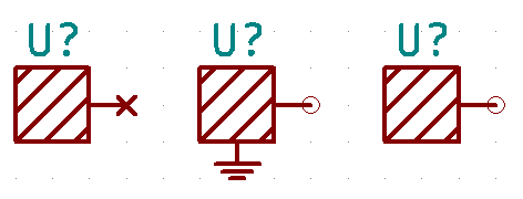
The Thermal Pads are represented on the schematic as:

I have not tried to use these yet as i have some doubts such as:

  • Is the pitch of the Thermal Vias too low (1.00 mm)?, examples on the web usually refer to 1.20 mm pitch which is quite a large difference at this level.

  • Would there be too many Thermal Vias at a pitch of 1.00 mm? Solder wicking problems etc.

  • Are the Paste Pads too small/too many?

  • Is it good practice to have seperate Thermal Pads or should they always be integrated into the Land Pattern?

Thanks,
Steev

1 Like

If I understand your proposal correctly, you are splitting the thermal pad from the footprint of the component. You are introducing a new component, the thermal pad, to be connected seperately in eeschema, which I like. And then you would have a set of footprints for thermal pads of different sizes.
Is this what you are proposing or have I missed the point completely?

What do you do if the thermal pad has internal connections in the component U?

m

@mifi: Yes, you are correct. I would split the Thermal Pad from the component Land Pattern where possible.

Regarding internal connections between the thermal pad/component, i change the pin(s) on the component symbol to electrical type N.C and name it/them to “EXPP”. The Thermal Pad Symbols/Land Patterns use pin #1, so as long as pin #1 of the Thermal Pad is connected to the correct net (GND or whatever. The net being the one that would have connected to the pins that are now N.C) the correct connection is made.

So in effect, the Thermal Pad “pin” replaces the component pin(s) that represent the connection to a Thermal Pad.

That would be a lot of work for the maintainers of the footprints, but apart from that… I have to think about the other consequences of your idea. I have been struggling with issues of NC pins en EPads myself lately when I was developing a component and footprint for the MAX9814. You can read that here, if you want.

The problem was that, so called, NC pins and Epins are to be connected in this case, despite their NC-ness.The solution I arrived at is to introduce all the pins in the component as non-hidden, forcing the user of eeschema to connect them.

Your solution, by contrast, is to remove the Epins from the component altogether and leave it to the discipline of the user to introduce them as a separate component, much like a heatsink.

It is an interesting idea, but I have to think about what that means in practice. Not all chips would need heatsinking, for instance, but do have an Epad anyway, because it is a standard housing used by a vendor. So now the user of eeschema will have to introduce a thermal pad in cases where no heatsinking is required. That is asking a lot of discipline.
Hmmm.
Suppose a component is manufactured with different housing options. When one changes the footprint, the user would then have to introduce or remove the thermal pad by hand. It is certainly doable.

m

2 Likes