The pad looks large enough that you should break up the solder paste anyway. I would remove the solder paste layer from the main pad (but leave the soldermask aperture) then I would add 4 rectangular pads within the main pad (all with the same number ‘49’) with an active paste mask. You still won’t quite get the visual result you want - your 4 innermost vias will still be completely covered by paste and the 8 outer ones will be half covered. This is all a natural consequence of your design - there is no reason to expect the vias to be exposed when you have instructed the software to put paste over them.
I’m new to QFN packages, but an old friend of mine (that recommended the article) is using them a couple of years and have warned me about possible issues.
I also used to follow the footprints provided in datasheets, but in case of QFN, following them can cause some issues. For example, following the TI datasheet’s recommend stencil will inevitably left some pad vias exposed to solder paste.
So, depending on the amount of solder paste that were applied two problems can arise. If the solder paste layer were too thin then your board can end with voiding as showed in the Rx below:
In the other hand, if excessive solder paste where used, then you can have problems with solder wicking variability:
Or can be a bit worse and end up with solder protrusions on the pad vias as stated in the image bellow:
I played a little bit and created a footprint using smd 10 pads with F.Past layer only.
I will try to use it in a new prototype soon after receive the board manufacturing ok first, of course
humm I didn’t use any solder mask over the main EPad… (I mean the main EPad was free of mask, copper in view)
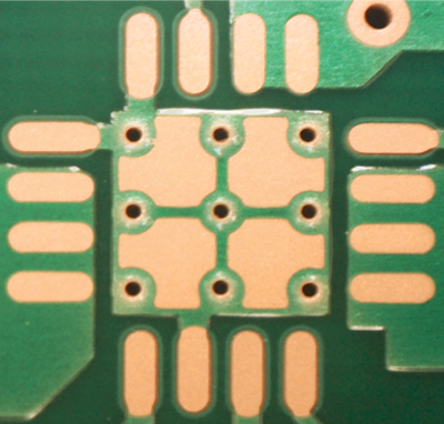
In your chip is there a big pad connected to vias? I don’t see it on your first picture
[quote=“maui, post:17, topic:5293, full:true”]In your chip is there a big pad connected to vias? I don’t see it on your first picture
[/quote]
That is the chip I’m about to use:
Let us know how things go when you do another run. I guess leaving the solder mask within the pad helps prevent migration of the solder (especially down the vias) but shouldn’t otherwise interfere (typical soldermask thickness = 0.012mm). Typical manufacturer recommendations I’d seen suggest that a 30% contact surface is what they aim for.
Looking at all those pictures… in the end the solution will be to have a raster of BGA like solder pads interleafed (half pitch) with a grid of vias.
No messing around with special pad shapes etc.
Just make the BGA thermal contact pads as big as you need to get 50% contact area and wetting/contact should be no big deal as the gas/air can escape into all directions.
Something like a 2D NaCl crystal cage.
Maybe the pads can even be simple squares, to get more thermal conductive area out of it (45 deg rotated).
Anything more complicated than that is begging for trouble IMHO.
Those X-Rays look like air/gas trapped within the solderpaste and not being able to get out during reflow.
I think that those pictures alone without a good context maybe do not reflects its real purpose, perhaps would be better read the article where they came from. There you will find more complete explanations.


