Very first KiCad project, please check my Gerbers

Hi,
This is my very first KiCAD project, derived from another work.
While I have thoroughly checked every connection and am confident in my design,
I am inexperienced with fab processes.

Can someone check if my Gerbers are OK and complete for a manual soldering at home?
Are all required files present?
All drills file, all mask files, for a production leaving my solder pads and holes free ?

It would be very nice if someone experienced could take a look before I order and get rubbish.
:grinning:

a BIG thank you for that.
Laszlo

https://github.com/rin67630/Drok-Juntek-on-steroids/tree/main/Hardware/KICAD/GERBER

(C7 is a radial condensator that will be soldered horizontally, I was too lazy to make a footprint).

C7 and J7 have crashed into each other!

At least move the silkscreen texts to free areas. There’s plenty of room.

1 Like

was specified, didn’t you notice it?

I also had a look at the project…

First thing I noticed were a few stray wires on the schematic:
South-East of JP1:
image

… and through both R15 and R20:
image

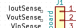
Then there are unconnected labels near J1 and J6:
image

And when running the ERC:
image
I get the “Pin connected to other pins, but not driven by any pin”
These can be fixed by adding PWR_FLAG symbols to your schematic.

There are some wires drawn though labels while there is plenty room to separate them, and this makes your schematic harder to read:
image

I’m also not a fan of those dashed lines. Usually they confuse more then they clarify.

Apart from that the schematic looks relatively neat. You even used the “No Connect” flags and probably have used the ERC.


The version I got from github complained about:
image
So I clicked on [ Yes ] to restore.
The version I’m reviewing may be slightly different from your latest revision.

DRC finds three errors:

It also finds two unconnected pins. All related to J61.
I got rid of both the errors and the unconnected pins by rotating J61 by 180 degrees. I sort of assume you already are / were aware of this.

I also do not like to draw zone boundaries on top of Edge.Cuts, and on top of each other.
I much prefer to make the zone outline look weird (such as pentagonal). This has three advantages. First, a zone is easy to select. and second, If anything goes wrong during Gerber creation, you see it immediately when inspecting the Gerbers.
Third: It’s easier to draw. No need for precise coordinates.
Something like:

Then I got the Idea to go back and do: Eeschema / Tools / Update PCB from Schematic [F8] and … oops. Your schematic and PCB are not in sync:


After the "Info: " lines, a bunch of "Connect: ", "Add: " and “Reconnect”. I cancelled this. I do not know your intentions, but schematic and PCB should be in sync before you make Gerbers and send them to be fabbed.
It’s also a good Idea to make a checklist with such things. Then, whenever in doubt, redo the checklist before you send out the Gerbers.

Your PCB is missing the KiCad logo. There are plenty to choose from :slight_smile:

Just out of curiousity what would change, I did the Update PCB from Schematic [F8] thing. It added the missing footprint for fiducial FID2, but it did not cause further DRC violations. So It’s probably just some renamed nets or similar.

Then the GND plane…
This is a simple design and a GND plane is not terribly important, but still, ESP32 runs at 100+MHz and I saw a reference to an ADC1115 module. Which is a 16 bit ADC I believe (have not checked the datasheet).
Such is enough reason to take care of your GND plane, and getting into a habit to do the GND plane properly will make you a better PCB designer.
High frequency stuff such as switching logic adds a lot of noise all over a PCB, and this can be easily picked up by the ADC. You do have some smoothing capacitors (C1 through C4), but their location is far from optimal. Ideally you put these capacitors physically in between the connectors, and connect the other side of the capacitor directly to a clean area of the GND plane.

You are going from connector J21 (left) to J4 (middle), and then you add a piece of track to go to C3 (Upper Right corner):

Your row of capacitors may also look nice, but they’re quite vulnerable at the edge of the PCB. If you put them somewhere in the middle, they are protected from fingers and stuff bumping into them.

You’ve clearly chosen to make rows of your resistors for visual reasons, but this is quite bad from an electrical point of view. It complicates the routing and with that you cut what should have been your GND plane into little pieces. Having some pieces of copper connected to GND on one side of the PCB and also some on the other side do not add up to a GND plane.
GND planes are pretty complicated things (Yep, they are) but you can do it quite decent with a few simple rules:

  1. Use (as close as possible) layer dedicated as a continuous GND plane. Ideally that layer has no interruptions at all. small holes from via’s and THT footprints are acceptable, but not long tracks which cut the GND plane to pieces.
  2. Analyze how currents flow through the GND plane. Keep sensitive analog stuff far away from switching digital stuff. In your case it’s ideal to put C1 through C4 close to the GND pin of the ADC1115 adapter, then route the signal from one connector to the capacitor, and then back from the capacitor to the other connector.
  3. One GND plane is enough. It is not very useful to also add much GND on another layer. One good GND plane is much better then two layers, each with 3/4 GND.
  4. If it’s not possible to make a good GND plane, then at least stitch the pieces together with via’s (as a last resort option).

Your PCB will work (concerning the GND plane) as is, but you’ll probably pick up more noise then needed for the ADC.

Silkscreen text of “J4” and “C4” is overlapping. The line from J4 also overlaps with the text of R20 and R12. The J21 text is also overlapped with a line. Such things are easiest to view when you turn off all other layers, so only one Silkscreen layer is visible:

Your I2C lines do not have pullup resistors. These are mandatory. They may already be on the adapter boards, but sometimes those are quite weak. If you add them to your project too, then you can mount stronger pullups if needed (depending on bus capacitance).
I’m out of motivation for now. I have not looked at the Gerber files themselves.

[Edit:] Removed a faulty screenshot.

3 Likes

Wow!
You took so much time to help a rookie!
I did not expect that level of support. I am overwhelmed!
THANK YOU!
Yes, I had originally rotated J61 and that made a lot of trouble.
That is the very reason for the errors in the check. I don’t know how to get rid of them.
The PCB should be OK nevertheless.
I have followed many of your recommendations.
I replaced the unconnected labels with plain text, that was definitely wrong!
The optimizations of the layout replacing all components will be for the next version. The device is running slow signals with some of them coming over comparatively long wires outside the PCB. The last optimization on the PCB could be somewhat overkill.

The silk collision on C7 is known: C7 will be placed horizontal to fit under the ESP32 which is plugged on the headers over it
I just missed a proper footprint for this situation.

Just replotted the corrections and uploaded to Github.

I hope I will get your advice, if the Gerbers are OK for ordering my prototypes.
I was worried if they are enough to drive a PCB that gets usable.

Regards
Laszlo

A couple of small points just relating to the cosmetic on the schematic

  • Near JP1 you have a stray wire.
  • C7 - Move label top top left so it doesn’t clash with GND (And then looks the same layout as labels on other caps)
  • This might just be me, but J7 I would orientate so pin 4 (GND) is on the bottom. Its standard practice (I think) that GND isd always on the bottom and makes the schematic easier to read.
  • The wires going from J21 to J4 - try and make all the wires as straight as possible without too many bends and it makes it easier to read the schematic.

Something like this:

Instead of:

On the PCB:
C7/J7 silkscreen is killing my OCD. :slight_smile:

1 Like

C7/J7 silkscreen is killing my OCD.

I know. I just lack a 3d model /footprint of a horizontal condensator with radial wires.
This rendering (without 3D for the cap) may be less shocking:

Moving the 3D model is also done quickly:


image

The “air wires” look stupid, but otherwise this would be pretty accurate for mechanical work.

But I just couldn’t stand the false silkscreen, I would take two minutes to modify it just enough to be enough…

image

Thank you for all that valuable stuff. I am still learning…
But could someone take a look at the Gerbers, if they were OK for a production, even if my current aesthetics are not state-of-the-art?

Is everything needed to produce a PCB for manual soldering present where it should be??
Thank you.

For me the workflow is to use the 3D view first to see if there’s anything suspicious. In this project it looks good, I don’t find anything wrong except that moving the silkscreen texts isn’t aesthetics only, it’s better to move them away from the bare copper, even though there’s an option to cut them off when generating gerbers.

You don’t need the paste layer in the gerber set at all because you don’t use a stencil. It’s better to not give files to the manufacturer which they never use or need. Having those files may only make things slower and more difficult for them. They also don’t have any use for position files because you do the assembly yourself. And this is essentially your file:

FID1      Fiducial  Fiducial_0.5mm_Mask1mm     7.6200    33.0200    0.0000  top
FID2      Fiducial  Fiducial_0.5mm_Mask1mm     7.6200    33.0200    0.0000  top
FID3      Fiducial  Fiducial_0.5mm_Mask1mm    55.8800     7.6200    0.0000  top

It wouldn’t be very useful for installing components, would it… :slight_smile:

Some manufacturers want repetitive data, for example drill files and drill map, because they want to serve you by checking everything twice manually. But only the actual drill files (most probably in excellon format) are needed. I would not add any pdf of ps files unless the manufacturer has asked for them. You can use the drill map file yourself to inspect it visually to see if it looks OK.

Basically you (or the manufacturer) need only the copper layers and the mask layer. And the silk layers if you want it in the board. That would be 6 gerber files. Then you need one or two drill files, in this case one should be enough because you don’t have non-plated in the board.

But there’s something going on in the drill files. There are three files, and only the PTH file has all holes, including the via holes. Delete the files, read the manufacturer instructions, generate only the needed drill files with correct settings.

In any case you should read carefully the instructions from the manufacturer and follow them. We can’t know if the gerbers are OK for the manufacturer you will use because we don’t know what manufacturer that is.

2 Likes

Sometimes I exaggerate a bit and you’re free to sift through my ramblings and ignore those parts.

If you want to rotate a part, then first rotate it in the schematic, and then update the PCB, so they both use the same netlist.

If you changed anything on the PCB, then delete all gerber files, and create a new set.

When I’ve finished a project I usally archive it with the same gerber file set that is used to manufacture the PCB, and a .pdf (.svg may be better) of the schematic, so it can be viewed without KiCad. .svg files can also be rendered directly by any decent web browser.

1 Like

I appreciate every advice. I am just still learning, and you help me to do it faster…
THANK YOU!

I gave eeliks post about gerbers a “like” for you.
His remarks about the gerber files read as spot on.

Thank you, i have removed the fiducials and the useless layers.
I believe the Gerbers are now good enough to jettison my first order.
I was baffled how cheap that order was at JLCPCB!
I suppose it was the just bait for the first order?

JLCPCB has somewhat confusing Capabilities table (which manufacturer doesn’t?)

In general they seem to be capable to do 0.13mm gap. However, they have this:

Your design violates this.

In any case it’s not recommended to go as tight as possible unless it’s necessary. 0.2mm clearance and minimum width would be better, more manufacturers are capable for that. Do you have real space restrictions?

1 Like

Call me stupid, but where can i set the minimum gap?
It should have been on the board setup, but I did not find the setting.

Pcbnew / File / Board Setup / Design Rules / Net Classes
I see that you already have a “default” and a “thick” net class, and assigned different rules to them. So you at least found that menu once :slight_smile:

I just had a closer look at what the project actually does and I find it quite a fun project. I have not looked at the firmware yet, but am tinkering now with the PCB.

My first goal was just to have some fun and thinking about how I would do the layout, and in the meantime I’m also making the design rules a bit bigger.

I’m not sure if you’re interested in this. but I’ll post my tinkering in a few hours. You’re free to ignore it of course.

1 Like

Hi paulvdh,
you are very warm welcomed “on board” (if I can say so in a KiCAD forum)

You might want to take a look at
https://github.com/rin67630/Drok-Juntek-on-steroids/blob/main/Hardware/JuntekOnSteroidsTTGO_PCB%26Patching.pdf
which shows in the last slides how the PCB adapts to different host DC/DC converters.

Everyone tinkering halfway seriously should have a programmable power supply.
Mines are programmable remotely from Honolulu or Ulan-Bator… :grinning:
And gives you tons of statistics…

We are discussing this project on Discord: https://discord.gg/gcmSpHH3bX

P.S. if you want to tinker with the existing board:
The pinout of J30 is not fixed you are free to remap if it optimizes the layout.
J11-J12 could be advantageously replaced by 1 piece of 8 pin holes array replicating 1:1 J1, but it should remain at the west edge.
J21 and J22 are not fixed either, could also be a 2x5 holes array or anything else: it is just a patch field.

If you turn the board like this the air wires are barely visible: