PCB shape from enclosure STEP file

Hi, new to KiCad, trying to create a PCB edge to match an enclosure.
I found this post talking about FreeCad and StepUp, but the details are lacking, or I’m to daft to get it.

The post shows a STEP file with multiple parts, my STEP file when opened in FreeCAD shows only a single object in the tree:

Is there are current or more complete youtube or tutorial that shows how to extract a PCB edge from a STEP/STL, and I mean really end to end, install extension, activate extension, open STEP/STL, find PCB edge plane, export, etc.

WHY?

The link provided is to a SERIES of products by Hammon Mfg. An actual part drawing is available if an actual part number is selected:

RZ0250.pdf

All the required dimensions for a PCB outline/hole mounting are already in the Enclosure DataSheet.

2 Likes

Sure, minus the radius of the concave and convex parts.
But really, if stepup can be used for this, from step or dwg or pdf, why not, just need instructions?

So, what version of FreeCad were you going to download???

you need to uncheck the ‘Enable STEP compound’ option in FreeCAD Import/Export STEP preferences

1 Like

The information for both radii are present within the number as shown.
2.805 mm
3.225 mm
4.975 mm

1 Like

I did a download of the 3D model of the RZ0203 and opened it in FreeCAD, and I have separate parts in the step model. I turned off the lid to have a look inside. After that I went along and drew a sketch of a PCB inside it and made a pad from it:

Your post reads as if you want to extract the PCB size directly from the step model. I’m not certain if this is a good approach.The sketch I drew of the PCB has a loose fit now in the enclosure, but the sketch is parametric, and therefore sizes are easy to tweak. Just double click on the PCB Sketch in the tree to edit it.

When you’re happy with the fit, exit editing of the sketch and:

  1. Select the sketch in the tree.
  2. FreeCAD / File / Export in the file format Autodesk DXF 2D (*.dxf)
  3. Create KiCad project.
  4. Set the grid to something coarse. For example 5mm.
  5. Pcbnew / File / Import / Import Graphics
  6. Choose “Interactive Placement”, and set the “Graphic layer” to Edge.Cuts"
  7. Pcbnew / Inspect / Measure and verify that the sizes are correct. As far as I know there are no units specified in .DXF files (Or they’re optional) and this leaves room for errors to creep in between metric and those other units.

2021-09-08_Hammond_RZ0203C.zip (1.1 MB)

2 Likes

There is a 2D DWG file available at that link.
Try loading that file into your favourite 2D CAD program and save as DXF e.g. QCad.
Or find an online converter.

DWG is autocad propriety format and I can’t open nor view it.

And it probably has the size of the enclosure itself, and not the .PCB that fits in it, so you still have to draw that yourself.

An alternative method is to take a screenshot from the .pdf


And then import a screenshot of it in the image workbench in FreeCAD. FreeCAD can calibrate those images, which makes it easier to copy measurements from the image into a FreeCAD sketch.

You can open DWG files in many freeware programs such as QCAD and FreeCAD.

Then still the issue remains that the drawing is of the enclosure, and not of a PCB that fits the enclosure.

DWG files are also not parametric, and therefore it is not very useful anyway. Working from a bitmap that has some measurements in it would be on the same level.

And I tried. FreeCAD does not understand that particular version of .DWG file. LibreCAD does not open it at all.

Qcad & Librecad tend to be buggy and/or incomplete. About 5 years ago I thought of buying Qcad (for a fair price of around EUR50). I did run the trial version of the commercial variant, and that seemed to work a lot more stable. In the end I did not buy it because my interest are in 3D cad.

I would also have to learn the program from the ground up. I was hoping it was pretty similar to the old autocad interface, but my knowledge of an 30 year autocad version did not help much.

Interesting. I have used a few Hammond cases. I actually use a 2010 version of Autosketch, a re-branded product bought by AutoCad from Drafix quite a while ago.
It’s much quicker to draw in than Autocad style programs.
To make a pcb outline from a dxf, I select the inner shell case lines, join as a polling then offset inwards by 1mn or so.
I’ll have a look tomorrow when I’m in my PC not my phone.
I would also like to remind readers that there are many versions of DXF & DWG. So when importing into Kicad use the oldest version available in your import/export software.

1 Like

What is the part you find

Because of FreeCAD I was introduced to parametric drawing, and I quickly got addicted to it. The old fashioned (such as Autocad) way of drawing pretty much resembles what is done on paper. You draw a line, and then you add measurements to that line. With some limited ability to stretch a line and create offsets.

Parametric drawing is … different. When you draw a line, it is just a line. After that you add “constraints” to that line. For example, you can make it a horizontal line. And then add another constraint for the length.

So it’s pretty much the reverse of what AutoCAD does. Adding measurements, add a number to the measurement, and that number is derived from the object. With parametric drawing, the number you type into the measurement is the definition of that constraint. The “stretch” function in autocad, is just typing in another number in the length measurement of the line.

There are also lots of other constraints. Such as mirrored items, lines of arcs of the same radius. Below a screenshot of the sketch I made for the PCB in the Hammond box. (the real sketch can be zoomed and scrolled. Download the earlier linked zipfile for more).

There are only three radii defined in this sketch.

  • 1.6mm for the four M3 screws.
  • 2mm for the eight corners.
  • 5mm for the inside corner cutouts.

So if you change any of those numbers, the others that are linked to it also change. This makes parametric drawing a dream to work with. Especially during the design stage. Designing a “thing” often requires many iterations of small changes. With parametric drawing you just click on any measurement to change the size of that feature.

The whole sketch just has 10 measurements, all the others are derived from those 10 numbers and geometry such as “horizontal” “vertical” “symmetric” etc. If you change the “19” in the lower left corner, then the upper right corner changes with it. (Because of “constraint 55” which makes two lines the same length)

And that is only the start of parametric drawing.
You can give names to measurements, and then create objects in different sizes with data from a spreadsheet or a script.

1 Like

just a mini tutorial for a fast modeling using StepUp in FreeCAD:

3 Likes

Thank you, this would make a great youtube tutorial to add to the plugin youtube collection.

That sure is a nice video of creating a PCB outline quickly from a STEP file in FreeCAD and it uses some functions I’m not familiar with (yet). But is it correct? And I’m missing context with the video. For example, why create a KiCad project first, before you switch to FreeCAD?

How do you verify measurements, how do you adjust measurements if the offset is not correct, or you need different offsets for the long and short side? Injection molded cases rarely have straight walls.

I created a parametric sketch from scratch, and it’s fully adjustable, and has the locations for the mounting holes. I also exported it to .DXF and imported it again in KiCad. (Verified it works, but had not posted that).

I am generally not a fan of such quick shortcuts. In my experience they need more fixing later on then doing it right the first time. But then again, for similar reasons I’m also not a fan of autorouters.

[Edit:]
It is not a shortcut. It just was a quicker and incomplete way to get the raw data out of the STEP file and into a sketch. Adding the misssing parts is done using regular methods, but this part was skipped in the video.

People vary, so choose a method that suits you.

But I’m intrigued enough by the StepUp workbench to reproduce the video, and I’ll do a writeup as I go.

  • 00:00 1920x1080 resolution makes it cumbersome to reproduce. Needs a lot of switching. If possible, making screencaptures of around 1200x800 makes the video’s easier to follow in a small window, so another program can run next to it.
  • 00:08 Setting the grid origin in Pcbnew… (See @00:37)
  • 00:12 Pcbnew / File / Open only exists in “Standalone Mode”.
  • 00:20 FreeCAD 0.20. Gosh, I’m still “stuck” on 0.19-24212-something. (No worries).
  • 00:23 Sped-up video races through menu settings. Not able to follow it without slowing it down (resulting in lousy framerate).
  • 00:31 Step import in FreeCAD.
  • 00:37 “Grid Origin is set in FC Preferences but not set in KiCAD pcbnew file” ???
  • 00:40 Turn off: FreeCAD / Edit / Preferences / Import / Export / STEP / [ ] Enable STEP Compound merge (I have it turned on, and it still works for me)
  • 00:45 Turning off unused objects such as lid and screws. (Spacebar works).
  • 01:01 Switch to KiCadStepUp Workbench.
  • 01:08 Select a vector. ( I choose a vector on the inside bottom, the top of the fillet, because that’s where the PCB will be).
  • 01:08 image KSU Tools “LoopSelection” Loop selection on a XY outline.
  • 01:08 Yah, that fails for my start vector :slight_smile:
  • 01:08 The inside corner of the top of the box works though. (Maui took the outside).
  • 01:14 image KSU Edges to Sketch. Select coplanar edge(s) or Face(s) or a single Vertex of a coplanar outline to get a corresponding Sketch.
  • 01:22 image KSU Offset 2D. Offset 2D object.
  • 01:28 Maui used “-2”. I used the default of “-1” because I selected the inside earlier.
  • 01:32 Select the newly created outline with the offset.
  • 01:36 image KSU 2D to Sketch. 2D object (or DXF to Sketch).
  • 01:44 Change the name of the converted sketch to something sensible.
  • 01:48 image KSU Push Sketch to PCB. (Make sure the right sketch is selected).
  • 01:54 Browse to an existing “*.kicad_pcb” and click [ Yes ] to overwrite it.
  • 01:56 Warning: Close your FC Sketch and reload the kicad_pcb file.
  • 02:00 Switch to Pcbnew. Load the “.kicad_pcb” file modified (overwritten) by FreeCAD.

~~ The End ~~

It all worked for me, and I could reproduce the video on my Setup@home.

Next step for me is that I’m curious what KiCad StepUp made of the sketch, so I examine it further in KiCad.

The resulting sketch in FreeCAD is underconstrained, with 53 degrees of freedom.
image

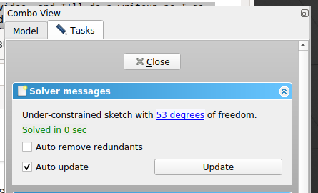
This is no wonder. as no measurements have been added.

So a little bit later I have a fully constrained sketch.
Wen fixing the missing constraints, you start with a very “wobbly” sketch. It’s easy to move vectors around, as nothing is fixed yet. So to start fixing constraints, start with important measurements, and make sure you accept the suggested numbers (which “fixes” them) without moving lines or arcs.

It does not have the mounting holes (yet) as in my previous example, but those can be added if needed.
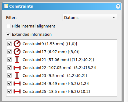
The sketch as just 7 “Datums” ( measurements with numbers). All the other constraints were satisfied by mostly making arc segments match with line segments tangentially (maybe this can be automated?) and a few extra’s, such as making arcs the same radii. Just normal FreeCAD stuff.
image

The resulting Sketch:

After measurements and constraints have been filled in, the measurements can be sanitized a bit. I changed 57.06mm -> 57mm 107.05mm -> 107mm and 9.49mm -> 9.5mm. This is done on purpose in a separate step, because the sketch is very “wobbly” at the start, and at the moment you enter a number , then it fixes that measurement, and adjusts some random other measurement to make it fit. So the order is:

  1. Enter “Datums” for important measurements (& accept what FreeCAD suggests).
  2. Add more constraints (“Horizontal”, “Tangential connections”, etc untill the sketch is fully constrained.
  3. Clean up the Datums a bit.
  4. Add further refinements such as the mounting holes if wanted.

I was wondering a bit about the origin of those “Roundig errors” though. On closer inspection I discovered that the inside of the box is specified as 109.05 * 59.05mm. (See earlier posted screenshot from the measurements in the .pdf file) The extracted data from the step file was pretty much correct (10micon deviation in X-direcion only). But remember, these measurements were made from the top of the box, and plastic enclosures never have parallel sides. The .pdf also specifies the inside dimensions at the bottom of the box (in the cross sections) as 108.22mm * 58.22mm. So there is still a loose fit for PCB manufacturing tolerances and easy mounting.

This is just one of my first serious experiments with the KiCad StepUp workbench in FreeCAD. I count over 60 icons in this Workbench, and only used a handful of them, so there is plenty more to explore.
image

Conclusion:
I just learned a new bit of FreeCAD and working with the KiCad StepUp workbench a bit, and it works quite good.
Big bunch of hails to all the great people working on Open Source Software.

3 Likes

because I’m using the push-pull MCAD collaboration pushing directly to the kicad_pcb file from the FC sketch. kicad stepup: the sketcher for getting to blinky

this short video is aimed to suggest a semi-automatic approach to create the sketch for your pcb.

The sketch I made is a canvas to add more features… but can gives you a first sketch to improve later in just few seconds.
Nothing blocks you to add all the constrains for your final user case.

The method in the video is similar to high level CAD sw approach in ECAD-MCAD collaboration:

The tools are working fine also on FC 0.19

if you watch my video, I have added a grid origin to the kicad empty board to give the collaboration a fixed reference.

this is really strange… if you load the step model with compound enable you get only a single object (compound) of all the internal models

nice… :smiley:

feel free to ask in case of needs.

I’m always in lack of time for producing documentation on my StepUp… it would be nice if some user would peek in to create tutorial in MCAD collaboration… I would be happy to help in case.

1 Like

I was writing down notes as I went along, and there was quite some overlap between me experimenting and your responding. In the end it turned out quite well.

Is there a way to automate the addition of tangential constraints the extracted sketch? This sketch has 12 arcs which each have 2 end points, so 24 constraints to be added for that manually.

With a bit of sanitizing the combination of your video and my writeup is pretty close to a FAQ article / tutorial.

here a way to add reference pcb holes… I added them as Dwg layer to be able to add later to pcb 4 mounting holes (I prefer to add holes as footprint instead of as Edge-Cuts)

1 Like