Hello, I am trying to panelize/combine three complex, unrelated shapes using something like mouse bites (vcuts dont work because tracing the edges would be absolute hell.) This is so that all 3 can be printed on one panel instead of having to make three separate orders, leading to saving cost on assembly (hopefully).
Anyhow, my question is simply how do I combine the boards such that separate three complex edge cuts are joined by PCB material w/mousebites. If there’s a better method other than mousebites let me know. I have tried finding similar issues, all I find are people panelizing small square boards, but I’m not doing that. I feel as if there has to be a better way
How is it used? Do I simply place it between the void of two boards and like magic they’re combined? If I have two squares and simply slap those between them I feel like it wouldn’t just work.
My experience is that it is all hand work. I place a mousebite where it is supposed to connect with de edge cuts. It does not automatically split the edge cut line. afaik that is not yet possible in Kicad? I manually fix the lines to fit this mousebite.
I might have to play around with it. If I were to place a square between two edge cuts, it appears as a separate square against the edge-cuts instead of a square combining the cuts. And if there’s even a little overlap the whole thing fails because of self-intersection. Mostly trying to figure out how to combine them, since if I can do that. I can place these and it should work just fine.
There are at least two different plugins that (claim to) help with panelization. Kikit and the sparkfun panelizer. I have not used them myself and do not know how well they work (or at all).
From left to right
Add the mouse bite
place it in position
Adjust the wire which runs through it and snap to the appropiate corner
add 2nd wire to fill the hole.
The problem with these plugins is that they were meant to panelize one particular board over and over, I’m trying to combine 3 boards using panelization techniques to then print on one board.
this looks interesting! I will take a gander, although I’m not sure which piece of the tool actually does what you say. Maybe GerberCombiner? Little to no usage instructions
I did a few panelisations in the past few years but these days with cheap shipping bringing the cost delivered per PCB to $0.7, it’s not worth my while. I don’t need 10 or 15 of a design, 5 suffices to blow up my components.
There are some designs that do require panelisation. An example is a SOP to DIP adaptor, you’d have lots of tiny boards if made singly.
Actually trying to dodge having to do 3 separate orders for 3 PCBs and save them some work combining them, and making multiple stencils… In the original post I mention 3 PCBs each of their own complex shapes. this saves on overall fab space and reduces PCB materials. I’m not trying to “panelize” more than I’m trying to combine.
It’s like placing a square and a circle on the same board, and printing them in one order, instead of two. Like a chip and a HAT for the chip. You get the idea. The fab calls them “Different Design” usually
They already combine lots of unrelated designs on large, typically 600 mm, panels. That’s how hobbyists benefit from the unused margins.Watch one of the many YouTube videos showing a PCB factory.
But you can ask them to combine shipping for several jobs.
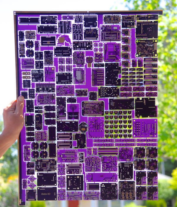
Indeed. And for those pooling services, they generally do not like to combine customer panels because their software has more choices and works better if it can combine a lot of small PCB’s then for fewer but bigger (rectangular) panels. And because of this you often have to pay extra for such panels. You do not save them any work. It’s just software that does the nesting. Below an example of such a big panel from Oshpark.
Oh interesting! I would have to play around with the edge cuts a lot because I have a lot of curves or very slight curves, at least. I think I’ve consigned to just put in a combined order of 3 things, I think places like JLCPCB combine those into one shipping
You can also let your PCB manufacturer do the panelization. Often you can then also order a stencil for the whole panel, and you can re-order the PCB’s from the same gerbers.
You can also download the Gerbers for the whole panel, so it does not even restrict you to go to the same PCB manufacturer if you want to order another batch.