I love the cheap Arduino Pro Mini clones for $2 and would like to build bigger things using them. So I buy the Arduino module and need to design a PCB with the Arduino and a bunch of connectors, for example.
Unfortunately, even after three days of searching, reading, trying out things and googling again I can’t find a way how to design a KiCad schematic module (the Arduino Pro Mini) that has several GND, VCC and other multiple identical pins (RX, TX) so that there’s just one pin in the schema, multiple pads in the layout and that the DRC and the whole Pcbnew understands that the multiple identically named pins are interconnected internally already.
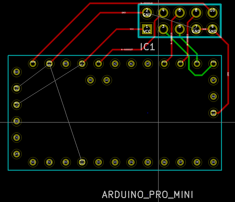
There are four GND pads and two VCC pads yet the Pcbnew does not understand that they are connected together on the Arduino module so it forces me to connect them on the PCB again. If Pcbnew saw they were connected it would even know that in the P1 above there’s no need to connect pads 2 and 7 because they get grounded via the Arduino’s interconnected GND pins.
I don’t want to live with DRC errors and incomplete routing. Isn’t there a way to tell the KiCad about the pins? I am sure there are many other components or IOs that do have multiple same pins… How do you tell Pcbnew to behave better, please?
I am afraid I don’t understand what you mean by creating “too plans”. I don’t want any pins to connect anywhere… I just want the Pcbnew to understand that certain pins are connected already inside of the module.
No, that wouldn’t work as GND and VCC of other components would connect to those virtual copper planes as well so the DRC would get confused the other way and I would be unable to add crucial GND/VCC connections of other items (the schema is not final, of course. There’s going to be several more components). With GND/VCC planes the router would optimize away any manual connections.
I doubt there’s a workaround for this IMHO common situation. I’d like to hear from KiCad developers how to solve this properly.
Add all VCC and GND pins to the schematic symbol as individual pins. Then mark all those you don’t want to have connected on your PCB as ‘no connect’ in the schematic. They will not be part of any ratsnest and will not connect to any copper pour.
madworm, even if I ended up with adding four GND pins marked GND1, GND2, GND3 and GND4 in the Part Library Editor and then, when creating the main schematic, had to manually choose which components connect to which Arduino GND pin (depending on where they’ll be on the PCB, which is IMHO bad practice to draw schematic according to the final - and at the moment unknown - PCB layout), it still wouldn’t address the main issue: that the GND pins are in fact interconnected on the module so I can use the GNDx-GNDy pair as an existing wire/path in my main design/layout/routing.
I am afraid that there’s no place in KiCad where this information could be stored when designing a module in the Part Library Editor, am I right?
I feel the need of something like a schematic sub-module where I’d draw a simplified schematic of the existing Arduino Pro Mini module (with interconnected GND pins) and then could use this sub-module in my other schematics so that KiCad’s DRC would see the GND pins connected together. Is the Part Library Editor in fact missing such feature or do I need to read more KiCad documentation/follow some KiCad tutorials?
Well, the stacked pin idea is mainly a schematic convenience. You are right, it doesn’t create internal connections between the stacked pins. It just allows you to have a cleaner schematic with one pin showing but all the stacked pins still get connected to the correct net. In the cases where I’ve used that trick I’ve always made external connections to each of the stacked pins in the layout. I sort of prefer doing that anyway (at least for complex parts) cause I don’t always trust that all the pins to the same signal have useable internal connections. There are certainly times when you want to take advantage of internal connections in a part and I’m not sure there is a good way to do this in KiCAD. One suggestion from a Google search is to give all the footprint pins which are connected together the same number but that doesn’t seem optimal to me.
Scott, glad to hear from someone who understands the issue. Yes, I wanted to take advantage of the internal connections in a part. Pity it doesn’t seem to be possible in KiCad.
BTW, giving all footprint pins the same number causes that they become unroutable (nothing can be connected to them in Pcbnew, the pins are crossed like if they were unconnected). So this is a no-go.
Why should it be possible for KiCad to automatically “understand” that the pins are connected internally? That’s really a very special case in PCB design. Normally, you wouldn’t trust that the internal connection has a low enough resistance and inductance to suffice for a proper connection, and there’s no way DRC can analyze it in any way either. The most common case for pins that are “internally connected” (such as IC ground pins, which usually all go to the substrate) is to still connect them together on the PCB. If you insist on not connecting the duplicates, don’t connect them in the schematic, and if you want to use them as connections in your layout, well, just don’t do that.
I didn’t want KiCad to understand something automatically, but I was searching for a way of explaining to KiCad that some pins of a newly designed module are connected internally. Like there’s the possibility to mark pins as power pins, data pins, floating, input/output direction etc. There it could just mark the connected pins and that would be it.
I have no single reason to NOT trust internal connections. The PCB of Arduino is well made and everybody relies on the fact that say all GND pins are actually GND, so they’re naturally connected together. Same for RESET, TX, RX and other “duplicated” pins.
If DRC were programmed so that pins of same name are internally connected it would be perfectly OK.
Your final answer “just don’t do that” doesn’t help at all.
I’m looking for the same functionality, and found this thread. I have an even simpler use case, for which I defy anyone to say “don’t do that”
I have an SPST switch, which has 4 pins, which are pairwise internally connected. This is a very common footprint for SPST switches. I just need to connect to either of the duplicated pins. Connecting them together on the board isn’t harmful of course, but completely unnecessary, and in this particular layout I’m working on actually quite difficult due to space constraints. Problem is that as it is, with a completely bog-standard use case, the DRC complains that I have an “unconnected” pin. And sure, I can customize the module for this particular use and remove the unused pins, but that’s poor band-aid solution that will break if the component is reset for whatever reason.
Let me answer my own question by myself: in the end I’ve created a new Arduino Pro Mini layout and assigned all the internally connected pins different names/pin numbers: GND1, GND2, GND3, GND4, RST1, RST2, TX1, TX2, RX1, RX2 etc. Then, when drawing a schema, I need to think how the final PCB layout will look like and decide which components to connect with GND1, which ones with GND2 etc.
Yes, it is a silly work-around and makes the schema unnecessarily complicated, hard to read and basically disables DRC. But the router does what I need and the final PCB looks good…
Bumping this thread because I have another excellent use-case: Coin-cell battery holders. They are, essentially, hunks of metal with multiple solder points for mounting strength.
Another good use-case: Fuse clips. Many have more than one pin, again, for mounting strength.
Do mainline KiCAD devs watch this forum? I’m already developing on my own fork at the moment, but this kind of feature seems like it would take a long time for someone like me (not intimately familiar with the code already) to try to implement.
They have 2 “pins”, each pin might have multiple holes. On the schematic you would have 2 pins as per the standard fuse/battery symbol. The footprint will have 2 pads, each of which might have multiple through holes. How you choose to draw that footprint is up to you. You might use one large pad with several holes, you might use several pads but they would all have the same pin number and belong to the same physical pin. This is already easily accomplished with KiCAD.
Even in the OP’s case of having a daughter board with several pins of the same name, I don’t see what the issue is. I do this all the time, currently I have a project with 3 boards each of which has a daughter board that plugs into it. As usual there are multiple power supply pins for these daughter boards. But I have never had any issues with this. I suspect the OP was misusing these pins in his design, using one GND pin for example, to supply ground to the board and another GND pin to supply ground elsewhere. I can see that causing problems but that is simply bad design. The multiple power and ground pins of a daughter board are usually intended only for supplying power to the board and should never form part of the ground path of any other circuit.
I don’t believe that KiCAD needs to change in any way to support some notion of external connections made by other boards.
I (the OP) can confirm the suspicion that I was misusing the daughter
board’s GND pins for creating kind of a second layer on my single sided
PCB where I needed to cross the GND through several signals and I
couldn’t route it any other way.
FYI, I solved it by naming the pins on the daughter board as GND1 and
GND2 and wired it in schematics the way I needed the PCB to look like.
It worked so well that I left the GND[12], TX[12], RX[12] and few other
pins in my copy of Arduino Pro Mini library since then. Granted, I have to
think a bit about the board design even when drawing the schematics but
it pays off greatly when routing the PCB.
When I do this with my battery holder, pcbnew doesn’t understand that the multiple pads are electrically connected and draws ratsnest lines among them and DRC observes it as unconnected:
Are you meaning to suggest there’s a way to not have that ratsnest line appear?
At one time I remember seeing an option to “Hide footprint ratsnest” but now I can’t find it.
I think most of us here are concerned about something called electromagnetic emissions.
If an electronic part has multiple gnd or v+ pins they should be connected to a power plane.
Yes a battery holder does not necessary need two V+ pins. (As long as the one connected can transport the whole current of the battery, In your example the trace looks quite thin. I hope the current over this trace does not exceed a few mA. Otherwise the voltage drop might be to much.)
If you want the second pin not connected to anything you can achieve it by changing the footprint. (Give it a different or an empty pin number. See for example Molex series 53398 connector mechanical pins)
It should never be the standard behavior that two pins with the same name are counted as connected if one of them is connected to the “source” of this “signal”. (how should DRC know where GND is connected to the power supply?)
I have some background in IC design. If i design an IC with multiple ground pins, the PCB designer needs to connect all of them to GND. (I would assume that they have the same electrical potential in all time instances.) Otherwise the IC might not behave as described within the datasheet.
DRC is strictly correct, they are same-net pads that are unconnected.
I have often thought it would be useful for PCB CAD tools to have a virtual-copper layer, that you could route that ratsnest on, ‘to keep DRC happy’.
The user knows they can use either pin, but DRC does not understand that, so some simple ‘jumper layer’ would allow designers to indicate what they know is OK, and DRC can find real problems.
I have exactly the same issue with switches and battery holders. In this case, using the internal connections would be perfectly acceptable and would make layout easier. I am not saying that it should be the default, but having it as an option would be great!

