Hi, new KiCAD user here and first post in this forum.
I created a board outline with mounting holes as a dxf and imported it using
File → Import → Import Graphics into the Edge.Cuts layer.
The problem: Traces are routed too close to the elongated mounting holes.
There should be some distance (e.g. 3mm) so screws and washers don’t cause any
issues.
I cannot find a way to define a keep out zone that is a fixed distance larger
than the mounting hole. How to do that? Any help appreciated.
I can draw the shape in CAD, if that’s of any help.
Yes, that helps.
Then make a custom footprint out of it and use your custom shape to make a pad in the footprint.
Note:
Apparently there is a bug in .DXF import in KiCad V5.1.5. This mornig I installed V5.1.6 but I have not checked yet if the bug has been fixed, but I assume it is.
How would a pad help here? I assume the user does not want to have copper there so it would neet to be a non plated hole. However the hole shape shown is not something that can be made with a pad (it is not a straight milling path but more like a banana)
@wxE5 possibly double check if a normal oval hole would suffice as the shape of your hole might indistinguishable in the final product from a straight milling that can be achieved with a normal oval pad. (milling in pcb production has rather large tolerances)
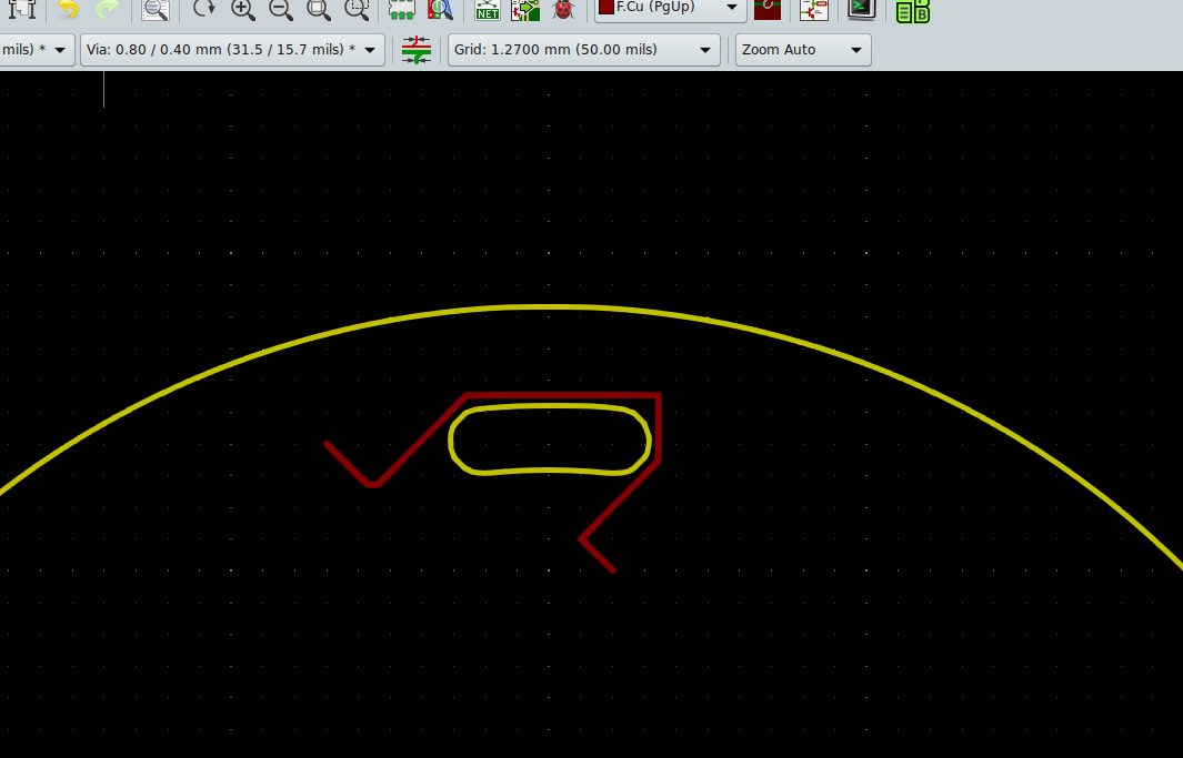
I can only hand-draw shapes using “Add keepout areas”. It doesn’t follow the original shape. So I will always include too much or too little space. And it’s hard to judge where the 3mm border is supposed to go. But that might be a workaround and I’ll play with that and see if that works.
This is how it looks (using a coarse grid to illustrate the problem that it’s hand-drawn rather than following the shape):
No, oval won’t work. It’a a round PCB. So it needs to have elongated mounting holes to allow adjustment after it’s installed. The shape and position of the holes is fixed and can’t be changed.
If there’s a better way to implement those holes, let me know. But since KiCAD doesn’t offer much drawing capabilities, I found it easier to import a dxf.
Another trick is to increase the thickness of your lines, this will automatically give you the added thickness as clearence, it just looks “different” with the “fat lines”
That seems to work (for traces as well as copper pours). Thanks for all your responses. So far I’ve gathered there are threesuggestions:
The built-in function “Add keepout areas”
This function is designed for hand-drawn polygons. It is usable to prevent
trace routing in the area. But it’s unsuitable to prevent copper pours
because the ragged hand-drawn line doesn’t follow the original shape and just
looks bad.
Creating a custom footprint for the hole
I started playing around with this, but it seems excessive work to create a
custom footprint for each hole. I was able to import the “keepout area” as a
dxf file. But I don’t know in which layer (KiCAD apparently doesn’t have a
keep-out layer).
So although I was able to import a precise keepout area (made in a CAD
program), I couldn’t get this to work. And it’s also not easy to properly
align the footprint to the actual elongated hole in the Edge.Cuts layer. All
in all this seems like a very laborious way.
As @der.ule has shown, one way which seemed to work, is to increase the line thickness. This works in pcbnew (although it looks awkward) and the 3D viewer actually shows the right PCB. However looking at the gerbers there’s a much larger hole. Here a few images how it looks in pcbnew, 3dviewer and gerbview:
According to gerbiew, the gerber’s hole is way too large. Why do the hole sizes in gerbview and 3d view differ? And -more importantly- how to fix the hole size in the gerbers?
However, normally, the Edge.Cuts layer is processed with the same router bit as such, the manufacturer will normally route on the middle of the line, but probably you have to clarify this with your manufacturer when sending your design.
StepUp has the option to push keepout area and/or fill zone from FreeCAD to KiCad… you can pull your board in FC, design your keepout area aligned to what you need and then push it to your K board.
@maui Thanks for the hint. I installed FreeCAD (appimage), added the StepUP workbench, managed to import the pcb. But frankly I know no further. I haven’t found much documentation.
The post KiCad StepUp WB: few enhancements suggests that one can create a sketch end export it to F/B.KeepOutZone. I have never seen that layer name in KiCAD, so can one create a KiCAD layer in FreeCAD? Isn’t it easier to create such layer in KiCAD (I didn’t know you could do that). Or maybe I’m misunderstanding how this works.
I created a sketch in FreeCAD but have no clue how to sync it to a F.KeepOutZone layer in KiCAD.
Even if I’ll manage to get it working, it seems like quite an involved process all in all.
It is the only one question from all yours I can write a word about. The tools to draw sketch in FC are more powerful than the tools to draw in KiCad. So in some special cases it can be easier to draw some complicated picture in FC then in KiCad. But I have never done it.
Since half an year from time to time I spend some time to investigate how to use StepUp. My today plan is to make a first try to do something with it, but I will try something different than you are asking.
@maui Sorry for the late response, I was afk for a few days. Thanks for having a look at the problem. I checked both files and it looks like it did the job. The big question is how?
How did you create the keep-out-zone (based on the pcb slot)? And how did you sync it with KiCAD? Those are likely noob questions, but this FreeCAD workbench is a very complex tool and I’m new to this.