How to define keep out zone in KiCAD 6

I created a board outline with mounting holes as a dxf and imported it using File → Import → Import Graphics into the Edge.Cuts layer.

The problem: Traces are routed too close to the elongated mounting holes. There should be some clearance to tracks and copper pours.

I asked the same question a while ago (How to define keep out zone) and der.ule posted a workaround How to define keep out zone - #7 by der.ule which I have been using since. The workaround was to temporarily increase the line width which would add more clearance.

But this has stopped working in KiCAD 6. How to achieve that in 6.0.2?

Version: 6.0.2+dfsg-1, release build

File > Board Setup > Design Rules > Constraints > Copper to edge clearance.

(If you need separate clearances for the board edge and the holes you can either draw lines on the margin layer or write custom rules.)

This affects also the outer edge, not just the holes, so that’s no option.

Definitely.

I’ve tried that. But I need to create each shape twice, once for the hole and then a second time for the margin. That’s much more work compared to the old version. And I ran into the problem that in contrast to the board edge lines, the inside of the shape is not ignored and filled with copper, see the example here:

It seems like that would be the way to go. How to write a rule that adds e.g. 3mm to the mounting holes but not to the board edge?

I’ve read the corresponding section in the manual but frankly, I have no clue how to write a rule to increase the clearance on my four mounting holes.

I got it working:


Here’s the rule I used:

(version 1)
  (rule "Clearance to cutout"
  (constraint clearance (min 2.8mm))
  (condition "A.Layer=='Edge.Cuts' && A.Thickness == 0.1mm"))

Then the real board edge was made a bit thicker so the rule doesn’t apply to the board edge. I could not change the line width of the mounting hole, but I’ll create another thread for that.

1 Like

A better solution is to use:

(version 1)
(rule "Clearance to cutout"
  (constraint clearance (min 2.8mm))
  (condition "A.Layer=='Edge.Cuts' && A.memberOf('mountingholes')"))

And then put the mounting holes in the group “mountingholes”.

First: I like your solution with the rule.

But one remark to the margin-solution:

I’ve tried that. But I need to create each shape twice, once for the hole and then a second time for the margin. That’s much more work compared to the old version.

you have not to draw a second “margin”-shape. You can copy the existing “hole”-outline to the margins-layer (better: don’t copy, use “Create polygon from selection”, this will set directly the correct layer) and change the line-width of the margins-polygon to 2.8mm.

2 Likes

I tried it and that works as well. Thanks for the suggestion.

I was going to suggest using a group, but I see you already got there. :wink:

(@mf_ibfeew’s solution is also a good one.)

1 Like

I adapted the solution to the following rule:

(version 1)
(rule "Clearance to mounting holes"
  (condition "A.memberOf('mountingholes')")
  (constraint clearance (min 3.5mm)))

This works fine for pours, but not for tracks. KiCAD happily routes a track through the keepout area (without DRC error/warning):

How to modify the rule so that routing tracks in that area is not allowed –or if that’s not possible– at least a DRC error is produced? I found the “disallow” keyword, but don’t know how to apply it to this case.
rule.kicad_pro (9.0 KB)
rule.kicad_pcb (26.5 KB)
rule.kicad_dru (131 Bytes)

As a last(?) resort you can draw a circle, use RMB on it, use Create from Selection context menu item → Create Rule Area. Press Del to delete the original circle. Now you have a circular rule area (keep out zone). This works even with other closed shapes made of arcs and lines.

This does not obey the clearance setting set in the rule, does it?

Select one of the mounting holes and one of the tracks and do an Inspect > Clearance Resolution… and post the results here.

I can’t, because the mounting holes are in a group and I can’t select the tracks when I entered the group. And when I delete the group, the clearance is different, that’s the whole point of having the group.

I had the files attached a few posts prior, so you can try for yourself. If there’s a way to select one grouped and one non-grouped component, please let me know.

I can’t, because the mounting holes are in a group…

Well, now that’s annoying. I’m not coming up with any easy solutions either. :frowning:

Anyway, the problem is probably that clearance is an electrical clearance, and a NPTH mounting hole has no electrical potential. Try hole_clearance or edge_clearance (either should work).

What’s funny is that I can select the group and the track segment, and the Clearance Resolution works:

Note how it’s “Circle on Edge.Cuts”. It looks like it takes the first item in the group.

And then for the zone:

Yet the custom rule works when filling the zone.

There are certainly bugs here.

I have tried that: hole_clearance only affects the hole and edge_clearance affects only the board edge. Using just “clearance” both are affected (the desired outcome).

[quote=“JeffYoung, post:14, topic:34662”]
Anyway, the problem is probably that clearance is an electrical clearance, and a NPTH mounting hole has no electrical potential.[/quote]

But the clearance works fine for the NPTH, here:


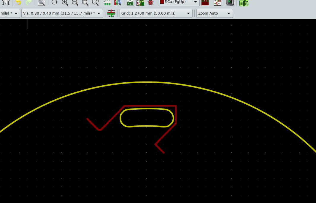
The problem is that tracks can be routed close to the mounting hole, in the area that should be kept empty. KiCAD is happy to route tracks in this area (and not even trigger a DRC warning). That is the actual issue here:

Should I file a bug report? Any other ideas welcome.

I didn’t notice before that one of your holes was just a circle drawn on Edge.Cuts. So you want to use both then:

(rule "Clearance to mounting holes"
  (condition "A.memberOf('mountingholes')")
  (constraint hole_clearance (min 3.5mm))
  (constraint edge_clearance (min 3.5mm)))

The fact that clearance is currently working is two bugs: one already fixed in 7.0 and the other that I’ve just fixed.

The actual shape is more complex, I just used a simple circle here for demonstration.

That actually makes it worse than my current solution. It doesn’t work here. To sum it up:

Using:

(version 1)
(rule "Clearance to mounting holes"
  (condition "A.memberOf('mountingholes')")
  (constraint clearance (min 10mm)))
  • The copper pour clearance works as expected. No DRC errors/warnings (as expected).
  • Traces can be routed through the keepout area (not expected) and no DRC error shown (not expected).

Using:

(version 1)
(rule "Clearance to mounting holes"
  (condition "A.memberOf('mountingholes')")
  (constraint hole_clearance (min 10mm))
  (constraint edge_clearance (min 10mm)))
  • The copper pour clearance works in general but show DRC errors/warnings when close to the board edge (not expected).
  • Traces can still be routed through the keepout area (not expected) and no DRC error shown (not expected).

Note that the DRC warning here is not the trace but the mounting hole. Remove the trace and you’ll still get the DRC warning. I need it the other way round. Mounting holes close to the board edge are perfectly fine and should not trigger a DRC warning. But I don’t want traces or copper pours close to the mounting holes.

So all in all this does not solve the problem of routing traces within the clearance area.

In the latest (self compiled) 6.99 (NOT 7.0 although Jeff said so!) there are no problems, it works now as expected. 6.0 is of course a different story.

Ok, thanks for confirming. Will this fix be included in the next (6.0.5?) release?