How create a STM32 Nucleo board for KiCad 5.99

Software developer and Beginner KiCad user here. I’ve followed the Getting Started tutorial, then created my own small dev board just for experimenting. Now I want to create a STM32 Nucleo board for the 100-pin stm32f105vc MCU of which we have plenty at work from old boards.

Now, how do I go about creating such board? The board exists in three variants Nucleo-32, Nucleo-64 and Nucleo-144. The nucleo-114 user manual MB1137 has a lot of information. Andh ere’s the schematic pack for the Nucleo-144. I’m thinking of having just 100 pin Morpho headers but keep the Zio (Arduino) header. stm32 nucleo-144 cad resources

What should be my next step?

  • Try importing those schematics into KiCad 5.99

  • Find an existing template for KiCad 5.99. I found this template for 5.1 but couldn’t use it from 5.99. stm-morpho-template. Is it possible to upgrade it?

  • I found symbols for Nucleo-144 in the MCU_Module folder and footprints in the Module folder. But that footprint is for the entire board, with all connectors and mounting holes. So far I’ve only used symbols that has corresponded to one component and footprints that has corresponded to one component. Are those symbols and footprints meant to be used on a carrier board for placing an existing module? And not for actually designing the module itself?
    image

  • Find a resource that describes the size and placements of the board outline and connectors. What is such resource called? Where do I find the existing dimensions? Should I use the measurements given in the user manual for the board? Or is there some more fool-proof way of obtaining the correct dimensions?

Normally I’d start with a search on github, but either I’m not awake yet, or they’ve removed the search button, which makes github unusable.

I had a look at the schematic packs from ST. It looks like it has a full schematic made in altium. This would be a good moment to experiment with the Altium importer in KiCad. (I have not used it myself, and it’s hidden in KiCad because it’s not developed far enough for … (Actually, I do not know in what state it id, as I wrote, I have not used it myself).

Another approach is to:


(I still have to cleanup that FAQ article)

If you want to turn the whole board into a KiCad project, it’s quite a lot of work. If you just want the PCB outline and connector layout, it’s fairly quick and you have enough to design a PCB that can mate with the nucleo board.

I made a KiCad project from the mobilinkd template for KiCad V5.1 and it worked after sorting out the strange 4 layer deep directory structure. When you’ve created a KiCad V5.1.x project, you can open it in KiCad-nightly V5.99 and continue with it.
KiCad templates are very simple (I like simple) It’s just a regular KiCad project with some meta info such as a description in html and an icon. Which means, you can dump the files from: https://github.com/mobilinkd/stm-morpho-template/tree/master/template/STM_Morpho in a directory, (maybe do some renaming) and then open it in the KiCad Version of your choice. This template does not have much info though. It’s just the PCB outline with connectors, and some empty connectors in the schematic. There are no labels with pin names, nor even power or GND. Combine that with that it’s for the 64 pin version and it also does not have the (horrible) “arduino” pin layout, and this template does not seem very useful to you.

Both experimenting with the Altium importer, and creating a KiCad project from the Gerbers seem valid options to get started. The Altium importer is the quiket if it works. Working with the Gerbers is almost certain to work. I did load the gerber files in Gerbview (It’s a 6-layer PCB) and it’ looks like it’s complete, but I have not exported it to a KiCad PCB.

1 Like

I had not looked at this approach yet while writing my previous post.

Those have both a schematic symbol and a footprint, and they can be used in both ways. The PCB footprint has nothing on Edge.Cuts, which means that it’s main use is for using it as a footprint in another project. The F.Silkscreen layer is apparently quite close to the real size of the PCB, so if you move that to Edge.Cuts you can use it as a PCB outline.

The schematic symbol can also be used in two ways. What it does for you is match the pin numbers with the footprint, so you have a reference how to connect stuff between the schematic and PCB.

Such schematic symbols and Footprints are a valid starting point. It gives you both the PCB layout with the connectors, and the links for all pins between the schematic and the PCB. I do not consider such symbols “comlete”. KiCad has quite good editors, both for schematic symbols and for footprints, and you can use the available library items as a starting point to adapt them to your own needs.

1 Like

I was doing something else, and then I noticed: Schematic Editor / Import / Non-KiCad Schematic and Altium Schematic File in the supported formats, which made me curious.

First tried the whole project, but this did not work, some trouble in KiCad with saving or renaming files (separate message for each sheet). So then I opened the Schematic Editor and did the sheets one at a time, and dumped them all in the same directory of a KiCad project, and this does work. I can now browse through the hierarchy, and all sheets of the schematic looks reasonable.

So I thought, I’d give the Gerber files also a try, and these are the settings I used during export to the PCB Editor:

Like in the "reverse engineering FAQ article I skipped paste and solder mask, and put the silkscreen on some user layers.

I’ll go further now to have a look of it works, just wanted to dump the screenshot here first.

18:28u I’m struggling quite hard now. for some *&^%$#@! reason I can only move stuff in horizontal, vertical and diagonal directions, and I can’t find a setting for this to undo it, and this is distracting me so much I can hardly get anything done, which annoys me even further. So I’m stuck in a feedback loop. At the moment I’m wondering if it’s some kind of user setting, or a bug in KiCad-nightly V5.99.

Pcb Editor / Tools / Cleanup Graphics finds over 1000 “zero-size graphic lines”.
image
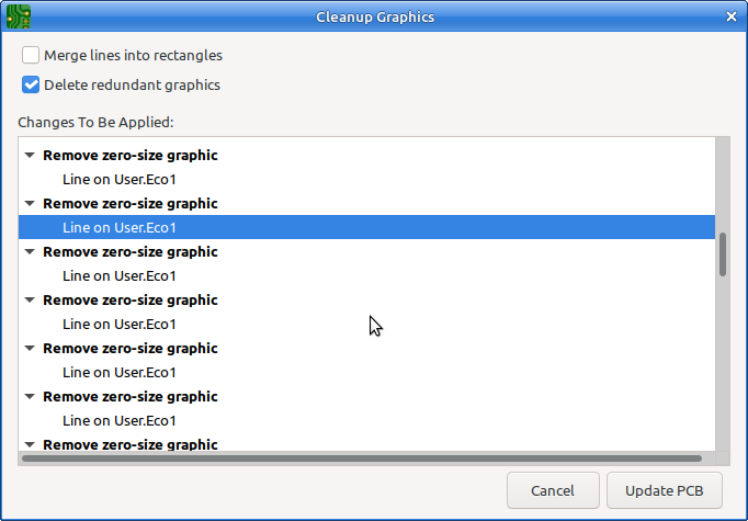
I’d thought to report it here before I delete them. (I also already merged a whole lot of lines into rectangles :slight_smile: Nice function.

While placing the LQFP144, I noticed that I could only get a good placement for 1/3rd of the pads. I remember something of bad resolution in Altium, (or maybe just in Altiums Gerber export). It clearly shows on the reverse-imported Gerbers.

19:04
I’ve seen enough to know that it’s doable. the user setting (or bug?) that limits movement to horizontal/vertical/diagonal is annoying, but I’m shifting a bit to cleanup of redundant stuff. For example, there is no footprint info, and It’s quite easy to replace the footprint graphics with real footprints. If you do this in the “dumb” way, it’ a lot of work. And I really mean a lot. Just the THT connectors CN7 through CN12 is: (20 + 16 + 30 + 34 + 2 * 72) * 6 layers = 1464 redundant polygons to delete, and that is just 6 connectors, so doing this manually is far from optimal.

It’s quite easy to delete the polygons in bulk with PCB Editor / Edit / Global Deletions, but then you also delete the zone boundaries which you want to preserve / recreate.

You can also first move them all with PCB Editor / Edit / Edit Text and Graphics Properties, to some otherwise empty layer and then Turn them off or delete them later.


I have lost interest to take this further. It’s not very complicated but just a lot of tedious work and I have no personal interest in it. It is also a very bad choice for a beginners project. It is a quite involved 6-layer PCB and it’s too easy to get lost. It’s also completely unnecessary. To make a PCB that can mate with this nucleo-144 you just need the PCB outline and connector layout, and can simply delete the rest of the PCB.

Overall, I’m surprised by the quality of the automatic import from the Altium schematics. Reverse engineering the PCB is quite a lot of work, and I only did it partially. I just assigned footprints in the schematic for some big parts such as the connectors and the LQFP144 and some of the 0603 resistors and capacitors which I could do in bulk, so a lot of footprints are still missing, and most are not even placed on the PCB. Currently this project has around 15000 DRC violations, so still some cleanup to do :slight_smile:

I advise to not try to take this to completion, but I post the partial conversion as an example of what can be done, and as a showcase of the Altium schematic import.

nucleo-144_2021-09-30T19:25.zip (2.3 MB)

1 Like

Thank you for going to such depths! Truly impressive.

Yeah, a 6-layer board is beyond what’s reasonable for me to achieve at this point. I did find this 2-layer Nucleo-64pins Kicad project for a 100pin MCU https://github.com/dmitrystu/nuco-v so I guess 2 layers is doable.

I downloaded your nucleo-144 project and I can see that the board outline and connector layout are contained in the User.Eco1 layer. Now if I remove the content of all the other layers, won’t this pcb still have a 6 layer stackup? Can I somehow copy just that Eco1 layer into another clean PCB file for a project that uses a 2 layer stackup?

If that’s too much hassle, then I might go down the route of modifying the nuco-v nucleo-64 project and just let some gpios be unused. Since I’m a beginner just replacing an muc and redo-the routing will be enough of an exercise for me.

I was just curious myself. Both for the quality of the Altium importer, and for experimenting a bit with a 6 layer PCB. I was quite surprised that most tracks are only 0.127mm thin and the tiny via’s and some other things too.

You can change the layer stackup in PCB Editor / File / Board Setup / Board Stackup / Physical Stackup, and then the small drop down list in the upper left corner:

image

Copying stuff in KiCad-nightly V5.99 to another project is easy. Just make a selection, then copy it to the clipboard and paste it in another instance of the PCB editor. You do have to verify yourself whether the data is correct though. Why not just use one of the Nucleo-144 footprints in KiCad?
As a beginners exercise you can use both, and then lay them on top of each other and see if they are the same, or add some measurements with PCB Editor / Place / Add Aligned Dimension.

The PCB outline in the altium project seems to be on almost every layer. All copper layers, Silk screen etc. and this is not how it should be done. I’m a bit disappointed in the quality of altium in this regard. Just as with the errors in the pads in the TQFP144. Errors are around 10 micrometer, but still a bit sloppy.

This topic was automatically closed 90 days after the last reply. New replies are no longer allowed.