Hello everybody,
I’m new to ngspice and I’m trying to learn how to create custom models.
I was able to successfully create and simulate CD4520B model by reproducing the logic diagram I found on datasheet.
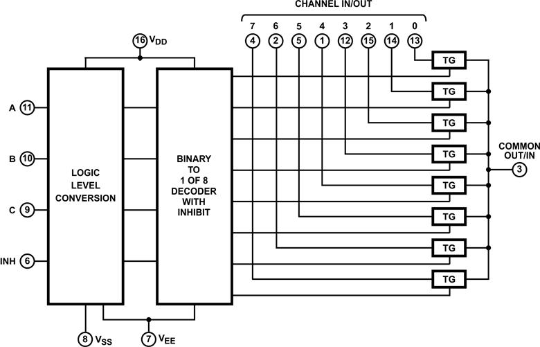
Now I wish to simulate CD4051.
I got the idea of creating two separate sub-circuits, one for the MUX and one for the DEMUX, implementing the logic diagram of the generic ones and choosing what to use based on an .IF statement.
Here is where I got lost, honestly I don’t know if this approach could work or if there’s a more simple way to do it.
Do you use KiCad/ngspice? If not, as this is a KiCad forum, please post your question at the ngspice user discussion forum ngspice / Discussion / ngspice-users. If yes, please let me know.
If you are using this for a digital application, then the switches are no big deal – on or off.
If you are using this for an analog application you probably want to look at a variant in LV cmos or something with better switches, and not the ancient metal-gate 4000 cmos.
As with all cmos analog switches, the switch is highly non-linear, having an N and P mosfet in parallel, and dependency on supply voltage and signal voltage. Tip: if you use it to set opamp gain, don’t put it in the feedback path (where the signal voltage varies a lot), but switch the other leg into a virtual ground to keep the signal voltage delta very low resulting in less THD.
Yes, I’m using KiCad and I love its feature of integrated simulator. I ran few simulations in the past with LTSpice, but never quite understand the mechanics behind it.
Maybe my question is more ngspice generic-ish but I saw that in this forum there’s also a section with a lot of great examples and I thought my question could have been useful to other folks out there.
I’m going to use it for a keyboard scanning matrix of 64 keys, having two CD4051B to handle row and columns respectively (as described here), so just simple control logic.
I will follow your suggestion and try to create a model with transmission gates.
You may need to set initial conditions.
The outputs are open. Why should they stay at 0V? There may be some tiny leakage charging the outputs.
The data sheet claims “break before make”.
You may need to set some decent W and L for the MOSFETs (check for the on-resistance).
I would put resistors to ground on all outputs – something like 10k. Never seems like a good idea to leave open nodes in a spice simulation.
The ancient CD4051 can run at 12V like you show but then all your logic needs to be 4xxx. If you run at a more typical 5V the on-resistance of the cd4051 switches is on the order of hundreds of ohms.
The old-but-still-good HC family or later LV-A family parts have switches less than a hundred ohms at 5V (but can’t run over 5V).
I am fond of the HC4051 as I used it for years to route I2C-data signals to 16 identical parts (that had no address pins) on two boards (the 86 is a jumper-selectable inverter for one of the boards). The i2c-clock can just go to all parts and then the i2c-dat line is routed by select lines. Since the dat is bidirectional, the analog-switch routing was ideal.
Initial conditions did not work (perhaps I was not able to set them properly…), but grounding all outputs with a 10kΩ resistor did the job.
The final adjustment of setting W and L for the MOSFETs made the simulation output look almost undistinguishable from the measurement with the oscilloscope.
This is what MOSFETs look line now:
To be honest I don’t know if these values are correct or they are totally out of sense, however the simulation output seems correct, so I’m happy with these models.
Just for trivia, how can I obtain the width ad length parameters from the on-resistance?
I’m not into ic design but I seem to recall something about p-channel devices sized larger than n-channel to make them perform about equally (lower mobility of holes vs electrons iirc). I would think if there was an ic application that would benefit from this it would be an analog switch with paralleled n and p mosfets. Perhaps someone with expertise in the area will chime in.
L/W is proportional to the on resistance. There are other proportionality factors (invers of carrier mobility which is roughly known) and gate oxide thickness of the CMOS process used (we do not know, but may estimate).
The MOS model used above has some default parameters for these to calculate I versus V.
You may take Fig. 2 from above, set the biases (voltage on input and output) accordingly to be on the NMOS on-side or the PMOS on-side and measure Ron for each bias.


