Homemade boards: NPTH connected on one side only

How do I tell Kicad “all through holes are not plated, with a pad only on the back side?”

My issue is that if I use filled zones over through holes, Kicad will think the two sides are connected, when in my case they are not (because I am unable to plate my holes or solder both sides of most TH components). I imagine this is common enough for hobbyists but none of the pad options seem to do what I want:

  • if the pad if “though hole”, I don’t have the option to select only one copper layer
  • if the pad is “NPTH”, I can select only one layer, but the pad gets disconnected from its net

The best workaround I found is to change them one by one into SMD pads for designing and changing them back for fabrication, which is very time consuming. Am I missing something obvious? Thanks!

I’m not sure if I got the real point of problem.
If you route only back side - it should be no problem that KiCad assumes top pads are connected with bottom.
If you route (tracks) at both sides than you would not ask that question (“all … holes…only…back”).
So I assume you route only at back side and at top you only want to add zone fill.
As you write that KiCad assumes top and bottom zones are connected that means you gave both of them the same net. So we can say - the only problem is that top zone really is not connected. You need to connect it in one place and - done (I skip the EMC subject and so on).
Oh… I got.
Zones are really divided into isolated islands and KiCad thinks they are connected.
I don’t know how to solve it but as separate subject I would suggest to add some vias. KiCad would think they are connected and your task will be to connect them.
In 80-th when we had no plated vias we did it following way. 0.7mm silver covered wire. Pinch 1mm of the end with the pliers and bend it 90 degrees. Cut a wire about 5mm from bend. Put that wires into all vias. Put a metal plate on the PCB and turn over. Cut protruding tips 1mm above the surface. Bend them and press them down with the pliers. Solder them.

Edit.
May be it was 0.5mm wire. There was a squeeze on it that it grew flat, which was probably why it seemed wider.

The issue is precisely that I can’t trust Kicad to tell me if I need vias. Because I mill my boards it’s convenient to start with everything filled (that I use as a ground plane, on both sides). As I route components they separate into more and more islands, and pretty soon it’s too hard to visually tell if they are all connected.

It would also be nice for tracks, I try to be careful to choose the right layer but sometimes mistakes happen - especially easy to miss after flipping one to the opposite side, because a track doesn’t have to start a new section every time it intersects a pad.

May be if temporarily use not existing net for both zones (you need to start with one hole connected to that net) you will be able to see which islands are not connected (they will be not filled). And when you add vias they will be filled. At the end you will have to change all those vias to GND.

That will work well once I learn how to design everything right on the first try :slight_smile: because the second time I would need to change each via twice. Since I typically have more vias than through hole pads it’s more work than temporarily changing those to SMD.

But thanks for the suggestion! Does this mean that NPTH pads cannot connect to nets, and not even a plugin or script can save me?

Don’t know. Never tried. Probably yes.
What about placing 3 pads one over another. SMD at top, SMD at bottom and NPTH?

Hi @UgaBuga

I’m not sure myself, but this fine member “calling” @BlackCoffee , I know, regularly frequents this forum and mills single sided PCBs.
Maybe he will see this post and comment. He hasn’t posted for a week, but maybe he will notice.

You could use long oval tht pads instead of round so you were able to solder the pins on both sides.

For small vias is more difficult but nothing forbids you to make laege vias so a wire can be soldered on both sides too.

I don’t see how that would work - I use SMD when I can, so most of my TH pads are for big things like switches, relays or connectors, they all tend to have pins that are miles away from the edge of the footprint, and they’re all plastic so they’ll melt if if I try to get the pin hot enough to solder with it.

And still, if I have 20 TH pads but need only a couple of them to connect on both sides I’d rather not edit each one and solder each one… and I can’t use Kicad to tell me which ones are the couple that matter.

Sorry, maybe I’m thinking too simplistically, but it seems to me you have two kinds of pads.

  1. Those for THT components you can solder both sides. In this case let it be a plated hole which isn’t actually plated because you are milling and the lead functions as plating after you solder.

  2. Those for THT components you can only solder one side. In this case you need to make modified footprints that have a pad only on one side.

Of course it’ll be a lot of work if you have lots of the second type, more so if they are mixed with the first type for a component.

How do I do #2? I am unable to figure that out. I can’t get holes that connect to a copper layer on only one side. That was my original question.

I don’t know if the footprint editor allows such pads to be created; obviously I’ve never tried. Maybe not as a TH pad but as a SM pad with a separate hole in it?

That’s a clever idea! but I can’t get it to work, because the clearance around the NPTH hole will cover the SMD pad (and for some reason Kicad really wants NPTHs to always be isolated from copper). Now I’m trying to figure out how to change that clearance setting - how do I do that since NPTH have no netclass? I tried setting the default netclass clearance to 0 and that doesn’t seem to affect it. Local overrides will not accept a negative pad clearance.

I wonder if you could create a pad with a copper free hole area in the middle for the drill hole but maybe the system doesn’t allow interior polygons. Ok how about a tiny channel so that it’s still one polygon. But this is getting too weird for me. :flushed:

Sometimes ‘my’ confusion arises from the different languages we speak so, I avoid reading too many posted answers and go to the original Question…
"How do I tell Kicad “all through holes are not plated, with a pad only on the back side?”

That said and, for my general need for using Kicad to output Gerbers I can easily use for CNC Milling, this is my approach:

• I Make the PCB layout without fussing or considering adding ‘Filled Zones’ as the PCB stock boards are Filled on one, or two sides.

• I set the Part/footprint Pad for Bottom (and/or Top) layers but, if Milling a Sigle-Sided PCB, I don’t often bother with setting the Top because (for single-sided) it’s only a Graphic in the 3D-viewer. Most of my custom footprints have only one-sided pads (Bottom). But, if using a Stock footprint, I may/may-not bother…

• NPTH un-plated: I usually Draw the Hole (or other shape) on either the Edge-Cut or User layers and Set them as a Contour in my Milling program (CopperCam). Just my preference… but can do it other ways.

• Understand that CNC milling will Route the Pad/Trace/etc Contours without User Needing to do anything special…

Example: I did Not fuss with this, I just grabbed some footprints and placed them on PCB and added some Traces on the Bottom. Added one Via. NOTE: You can see that ‘my custom footprints’ have bigger, oval pads (the crude small ones are Stock and look worse in Graphics than they actually are when machined. I LIKE BIG PAD’s. Oh, and the Graphic’s of the “Hole’s” does Not reflect that I use the Drill-bit I want but, I leave the Default holes size as-is…

Summary: No need for Filled Zones (the stock PCB has them, that’s why we use them (unless you want to do your own Cu Plating!)

RESULT’s in CopperCam

1 Like

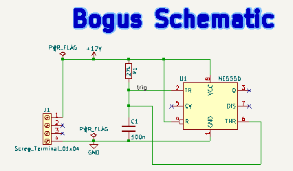
I’ve been tinkering a bit with an example, and I think I managed to get something usable. I first made a little bogus schematic, just to have something to put on a PCB:
image

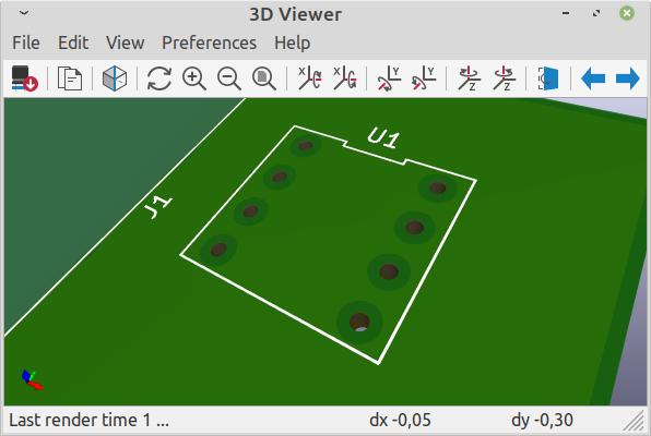
Then I designed a footprint for a DIP8, and I made pads with both an SMT pad on the bottom layer only and a NPTH hole. And then I put it on the PCB to see if it works. I also put a copper pour over the whole front of the PCB.

The front looks like:
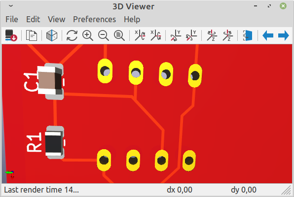
image

And the back:
image

With the way I designed the footprint, DRC is mostly OK with it, but there are has a few problems.
One problem is that the center of the SMT pads can not be reached, because it’s in the hole, and this makes it a bit difficult to connect tracks to the pads. A way to circumvent it is to first draw a track segment, and then move it over the pad (or just copy some existing track segment).

The other problem is with the clearance. DRC complains about the hole clearance. But that is relatively easy to fix by setting: PCB Editor / File / Board Setup / Design Rules / Constraints / Copper to Hole clearance to zero. After that change the only complaint by DRC is about some silkscreen thing for another footprint, and there is something with the schematic parity, but I have not looked into that.

I’ve attached the test project below, I hope you find it useful.

2022-08-02_asdf_Dip8_SingleLayer.zip (21.1 KB)

Some other things to consider:
KiCad can generate a “drill map” file, and this groups holes with specific diameters. You can make use of this by using specific hole sizes for specific purposes. For example if you want to make your own via’s and want to use those hollow staples, then use a specific drill diameter for that, and make sure that drill diameter is used nowhere else.

I made the footprint in KiCad’s footprint editor, but started with the wizard for a DIP package. Those wizards are quite simple (a few pages of code) Python scripts. If you want to continue in this way, then I suggest you make a copy of that script, and then modify the copy so it generates pads with all the right properties.

I can’t get rid of the clearance, and it’s not just a DRC problem, I can’t get the pads to connect. (Though I did set that setting to 0). This is what it looks like for me, I want pad 2 connected solidly to the fill around it:


image

What am I doing wrong?

  1. Download the example I made.
  2. Look if it’s what you want, test DRC etc.
  3. Modify the example I made. Do you encounter any problems with it I have not mentioned?
  4. Are there things you want differently?

The biggest advantage of working with that example is that I know what’s in it, (and anyone else can have a look too) so then at least we know we’re talking about the same things. A screenshot has much less info then a KiCad project.

your example does do what I want, but I can’t reproduce it on my own project. I will try to go through each setting to figure out what’s going on.

Good to hear (read) some confirmation.
I did quite some fiddling with pad settings to get it to something I thought you wanted. You should be able to compare the footprint I made with what you did in your own project.