The current issues, and clearance violations. I would like to know if there’s a way to segment a trace so I can move a section of it to gain more clearance. When I try to move now, I’m stuck on both sides. Adding extra points on the track so I can move a section of it, not the whole thing, would be helpful.
Curiously, there are no nets when I pour the copper fill and try to select what it should connect to. I’m not sure why that is. Didn’t run into this issue on the first PCB which I made totally in KiCad. The imported LTspice schematic for this PCB left me with numerous issues like this.

I had not looked at your routing earlier, but it looks like the usual wiring mess that is caused by a combination of bad footprint placement and an autorouter. It reminds me of a quote I read recently:
Good footprint placement is about 80% of a good PCB design, and that is before even the fist track is drawn. With good footprint placement, a simple analog PCB like this can usually be done on a single layer, so you can completely reserve the other copper layer for a solid and uninterrupted GND plane.
Yes, you can: select a track, then right click on it and select Break Track from the context menu. But it is a function I never use. An easier way is to just start drawing a new track, and when that track connects to a different section of itself, KiCad automatically removes the old redundant section. (This depends on PCB Editor / Route / Interactive Router Settings / General Options / Remove redundant tracks.
This is also behavior that can be greatly influenced by the Interactive Router Settings. I usually do > 90% of the routing with the Shove mode.
In the properties of the copper zone, you select a net name for the zone, and KiCad automatically creates connection of all the pads of that net which are inside the zone. In your screenshot you can see a few of these connections (created with thermal reliefs) in the upper right corner:

Note: You can remove all copper tracks for these nets (It looks like the GND net, which is good) Direct connection to a copper zone is good, zones have a much lower impedance then tracks, so the tracks are redundant. when you just rely on the zone connection, and remove the tracks for that net, you free up a lot of routing possibilities for the other nets. However, In your project, you’ve cut up the zone into a lot of barely connected sections, which greatly reduces the effectiveness of the zone.
These are all red, purple and turqouse herrings (Or anchovis).
The combination of bad footprint placement and autorouter spagetti just creates such a mess that you can’t easily recognize what else is going on. (Such as missing the GND connection to the zone).
Have a look at the section I highlighted below. It is a part of three nets, with the connection through C1 and R19. That single track goes all over the place, and it greatly reduces the options for laying other tracks. It is a classical example of the behavior of a simplistic autorouter, and exaggerated by bad footprint placement. (Or the other way around, bad footprint placement makes a simplistic autorouter behave even worse).

To make something decent of this PCB, you pretty much have to delete all tracks, then make a decent footprint placement (Hint: making nice looking rows of resistors is usually a bad strategy for achieving optimal routing). And once the footprint placement is done properly (this is the difficult part) then routing is easy. When you do the routing with an autorouter, you skip the iterative process that lets you improve the routing. Quite often, routing can be simplified by just moving a few footprints. And an autorouter does not do such things. It just creates spaghetti really fast.
1 Like
Detailed advice. Thank you.
As for that trace, outlined in green, now that I consider the path through the capacitor, yes, it is a cicuitous route. This is one iteration of many experiments, as I dip my toes into this new “art”.
Thanks on the ‘break trace’ command. It’s name led me to believe it would actually break the connection, not add points by which to reshape straight runs.
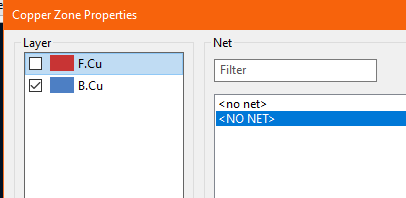
As you can see, my grounds don’t have any nets:
I suspect that was a problem I created by importing my LTspice design. I should have re drawn everything from scratch in KiCad, like I did with the relay PCB and everything would have the proper nets.
I was thinking of trying different methods for layout. This layout came from a plugin “Schematic position” which arranged the footprints in the general flow of the schematic (supposedly). They were an overlapping mess and I needed to move every footprint to make space between them.
My B+ lines still are separate (they should be common), so I’m guessing there are missing nets and the PCB editor doesn’t know how to assign them.

One of the issues I’m not sure I’ve done right is, since there are no B+ parts in the menu with voltages beyond 48V, I used one of those and changed the value to 250V… Other rails marked with that power connection should, theoretically, be connected in common in the PCB, but in practice, they came out separate. So the PCB ends up with two sets of grounds, and two sets of B+ high and low connections. Been scratching my head over that one for two nights now.
Not to be deliberately snarky, but how much time are you spending cleaning up the output of the autorouter? How do you even know what needs cleaning up?
More seriously, you are doing analog design, and there are many things to consider and learn about that will only come by learning and doing. Autorouters make more sense for complex digital design, and from what I have seen, their effective use also requires a lot of learning and setup in addition to already having a good understanding of layout techniques.
Also, be very wary of using LLM-based AI to learn analog design. Lately I have started to see “how-tos” and tutorials that are a dangerous mix of good and bad advice. If you are using a tutorial, it is because you don’t know the subject that well and this makes it difficult to separate the good from the bad, hence the danger. This is especially true when the good and the bad are completely interspersed in a reasonable-sounding manner.
John
1 Like
Well for me, I’m well versed in the design principals, coming from an RF design background some 45 years ago, but laying out components on a PCB requires a lot of spatial processing on my part, which in my octogenarian years has faded along with my eyesight.
On the first PCB, almost no time at all cleaning up the autorouter results, as they were better than my first manual attempt.
I’m mainly trying out the auto router on an experimental basis to see if it can get me past some of the hurdles. I have another plugin that places parts according to their order in the schematic. That can help a bit, but brings its own challenges.
It takes a great deal of focus to place parts and determine the least entangling routes for traces. If I could see better, it would make things a lot easier. Some of these tools can help make up for my physical and mental decline, at least I hope so!
Ok, that makes sense. It’s not a typical use case or user.
John
I also past 50 years a few years ago, and around that time I treated myself with a 107cm 4k monitor. (This also was the reason to replace my 13 year old PC, it was not up to the task of generating pixels for a 4k monitor). This is by far the best investment I made in the last 10 years. My eyesight is still quite reasonable, but also slowly decaying. I can’t see individual pixels anymore on the 107cm monitor, the “jagged edges” of text just blend into each other. I can hardly see a difference whether sub pixel rendering is on or off. I guess that in a few years time I’d have to chose between setting the fonts a bit bigger, or using glasses for the PC.
Before that I had a dual monitor setup with two 61cm (24 banana) monitors, and this worked quite well with KiCad. Having the schematic editor open on one monitor, and the PCB editor on the other monitor, gives a lot of overview with the cross probing.
You are not alone in this. The first handful of PCB layouts I did was in my youth years in the early '90-ies (with “ultiboard”), and this was a huge puzzle. It needs a few dedicated and trained braincells to be able to create a good footprint placement and take advantage of parts to double up as “bridges” to untangle the wiring on a limited amount of copper layers. And you do not train these brain cells by using an autorouter. Those first few PCB’s were quite simple, but the routing alone took several days of work. But after a while, you start to form patterns in your brain, and you gain the experience of how to do this much more efficient and quicker. I also tried an autorouter in those days, and I found it unusable. They may work for some sort of designs, they can even be essential to be able to route very complex designs at all in a reasonable time, but a simplistic autorouter is just a waste of time. It’s mostly a trap for inexperienced people who think they are “nearly finished” after the schematic has been created.
And actually, I find the puzzling you have to do to create an (almost) optimal PCB layout fun to do. It’s much better then doing sudoku puzzles. They end up in the paper recyler (or simply get erased when done on a PC or e-Book reader (the pocketbook e-readers have sudoku). If’ you’ve created a good PCB layout, you can have it manufactured, and make a project you can touch and use later on.
1 Like
On the first PCB, almost no time at all cleaning up the autorouter results, as they were better than my first manual attempt.
Not wanting to beat the dead horse, but this is always, always true. Everyone’s first PCB is terrible, awful, no good.
However, if you route the first one manually (and painfully), the autorouter is usually not better than your second attempt, because the autorouter is still as bad but you are much better.
It takes a great deal of focus to place parts and determine the least entangling routes for traces.
Again, always, always true. Placement is FAR more important than routing. Good placement makes good routing. Even godlike routing can’t fix bad placement.
A key early-stage tool for working out what is good and bad for routing is the ratsnest view. You can get a good idea of what will and won’t route easily from how many lines cross.
If I could see better, it would make things a lot easier.
Specific visibility hints
KiCad is fundamentally a graphical program and therefore the scope for visual accessibility is sadly a little limited, but that doesn’t mean we shouldn’t try. It does have some things you can configure for enhanced visibility if you are struggling to see things clearly.
The ratsnest lines are thin by default, and you can increase the line thickness:

This is the pic_programmer demo project with:
- all traces deleted
- in high-constrast/dimmed mode showing the F.Cu layer (H key)
- zone fills not shown, only boundaries

- thick ratsnest lines (you can change the colour and opacity on the right)
- grid set to be thicker (Preferences → PCB Editor → Display Options)

You can see the ratsnest has few crossings and more short lines than long lines, which is a good sign for routing.

You may also find setting a layer preset list to help filter out clutter, e.g. only F.Cu and F.Fab and no values may be to your liking. Set the layers and objects as you need in the right panel, then save as a preset, and you can select it with Ctrl+Tab at any time.

Also you can change the colour scheme if you find it hard to read - this is Monokai High Constrast:

Get this from the KiCad project manager, Tools → Plugin and Content Manager → Color themes:

And you can modify it as you want by creating a new theme (in preferences).
And of course if there are things that you find inaccessible and you thing they can be improved, please do raise a bug on Gitlab - avoidable accessibility issues are bugs.
4 Likes
Compliments on an excellent tutorial @johnbeard.
The “Specific visibility hints” section is worthy of placement in the FAQs.
I’ll do that later today.
Thank you. That is especially helpful about the rats nest thickness. I was having trouble seeing those lines!
Monkai them is a mixed bag… with filled ground planes, the contrast isn’t that much. It’s fantastic when there’s no ground plane though. I see I can easily switch between them.
What’s on my to do list;
1, find out why there’s no nets on most of the parts, especially grounds.
2. make a better placement of parts
3. find out how to assign larger trace thicknesses to power and ground traces, so that if I DO autoroute, the router will use the appropriate thicknesses.
Mainly, I’m enjoying the process of learning this new tool, and I’m experimenting with a lot of different means to the end result. If the board works out, I may release it as an upgrade kit in the future.
Netclasses is the concept you want to look into.
1 Like
If you draw (not copy from somewhere else) your schematic, each wire, when highlighted, will show its “net” in the bottom left of your screen.
See below:

The wire between R2 & R3 is highlighted (red arrow) and the Connection Name shows the “Net” (magenta arrow). If a Net exists here, when you go to “Tools” then “Annotate Schematic” then “Update PCB from Schematic” your PCB will show all the footprints and ratsnest lines.
If Nets are missing on your Schematic, you haven’t used “Schematic library symbols” or “wires”. Note; graphic Lines and Busses are NOT wires.
As @retiredfeline mentions, Use Net Classes. Find this at “Schematic Set-up > Project > Net Classes”.
If you set these up correctly, the Net class will show, when a wire is highlighted, at the bottom left of your screen next to the Net. See yellow arrow in above screen grab.
I’ve never used an auto-router, so I’m not sure if an autorouter will read and use the Kicad net class track widths. I have doubts if an autorouter will see Kicad net classes, so don’t hold your breath for that to work.
If Net classes are a bit much for you at the moment, at the top LH side of your screen is a button marked “Track - Use Net class width”. Click the arrow at the RHS in the box, click Edit: Predefined sizes and using the + sign at the bottom of the newly opened table, add some new track widths. This allows you to use hotkeys to change track widths on the fly.
1 Like
I bought a 32" monitor in 2008, a HP LP3065, which was a huge upgrade over the NEC 6FG that I was running prior. But everything got smaller due to the higher native resolution. But in 2011, I suffered a stroke and after that, I developed muscle paralysis in one eye, causing that eye to gradually become more rotated over the years, resulting in a most annoying double vision. The condition is a subset of Strabismus, called Cyclotropia. When I was diagnosed with it later in 2011, it was 3° tortional. Now it’s closer to 25°. I often have to shut one eye just to read text on the screen, as the second rotated image confused me. But then there would be a big ugly floater in my central vision. Or the other eye would be blurry. And at my last eye exam, they informed me I have cataracts. After my second major heart attack last year, my eyesight got drastically worse. I had another stroke while in the hospital after the surgery. This past April, I collapsed on the kitchen floor, was rushed to the ER, where it was determined I was bleeding internally. Lost 4 pts of blood. Stromal tumor in my stomach found to be the cause. Had another surgery to take that out. But the loss of hemoglobin further worsened my eyesight. And I can’t describe how bad the cognitive decline from being on Atorvastatin for a year. When I got off that drug, I was able to think again. My mind is still sluggish, but much improved over when I was on that drug.
Needless to say, I’m barely functional, mentally speaking, but I’m doing my best to do things in smaller chunks. I fasted for a couple of days in preparation for a colonoscopy I had this morning, and that helped somewhat with mental clarity.
You’re right about the puzzle aspect of footprint placement. I think if that can be optimized, then the routing will fall into place pretty much like magic. I am just very curious as to how well these autorouter tools can work. If there’s a way to get a job done more efficiently, I seek it out. But what I’m doing is experimenting with these tools to see what works best. Ultimately, I’m going to have to ‘strain the brain’ to play with parts placement with a goal of both optimizing routing and isolating signal and power traces for best performance. I know the importance of good PCB design. A lesson learned was in 2000, when I was working in broadcast engineering. I was building new studios for 7 radio stations in a major broadcast chain and we got the first digital on air mixing consoles from Harris Corp. “Impulse” was the name of the console and we immediately noticed white noise when testing the mic preamps. When I put an analyzer on it, we found that most inputs had a s/n ration of 38 to 40 dB! This was clearly a failure on the designers part to isolate digital busses from analog and the improper use of grounds.
Back in the 1970s, when I designed broadcast equipment, I had to consider RF rules for PCB design. I had a lot more working brain cells back then, but we did it with mathematics and paper mockups to plan out the best possible layout.
Ultimately, I’m going to rework this design many times, as I learn more of the features of KiCad. It’s been barely a week so far. To think I have been using AutoCad since the 1980s and Adobe Premiere Pro for video editing since the late 90s, and I actually went to school to learn to use a DVD authoring tool in 2003, called Sonic Scenarist. It took years to be competent in those programs. The fact that I was able to kick out a working PCB that passes DRC and passed QCC at JLPCB this past week with just two days of learning the program is testimony to the good design of the software, KiCad.
As I get into my eight decade of life, I seem driven to learn new things–it’s as if my brain knows it’s dying and is trying to save itself by pushing me into learning new software, Since I got out of the hospital in May, I’ve learned a new video editing software, DaVinci Resolve, and now I’m learning KiCad. I’m literally forcing my self to fight off dimentia, and I think I’m slowing winning the battle.
2 Likes
It looks like things went astray because I imported my design from LTspice.
As opposed to the relay board I made this past week being started from scratch in KiCad, which didn’t have these issues of missing nets.
I’m seriously considering redrawing the whole schematic in KiCad, so that all my wires will have nets and the PCB layout will have the correct connections. At the moment, I have nothing:

It appears I’ve got the other setting per your recommendation already:

I believe there is a way to assign net class for each trace being drawn, but I don’t know the hotkey at the moment–I saw it in one of many tutorials.
Then the next challenge is doing a mirrored symmetrical layout for a stereo preamp / driver circuit. I build one circuit and duplicate it, usually. Arranging the parts twice, seems like wasted work, when there may be a better way to make the opposite channel layout. But that’s partly why I’m doing this driver PCB project. I have the Dynaco sitting here and it’s a pet project to improve its performance while creating what could become a commercially available kit with the prestige of my amp repair company on it. I think I would sell a few, if the PCB turns out well and I can write a good instruction manual, drawing on my skills as a former senior technical writer at GDC Corp back in the early 80s.
Let say that I think you have come a long way so well done.
You can assign a netclass to a track, but better is to assign a netclass to a net or group of net by the net name(s).
2 Likes
Visited your site. I am 74 years ‘young’ after that!
Felt like a 10 year old kid in a candy store.
Here are some near to OEM specs round KiCad valve/tube pcb footprints to play with.
Plus a Polar/Cartesian/Euler Excel XLSX Calculator to plot coordinates and make your own.
KICADVLVMODS.zip (17.3 KB)
1 Like
The Track box allows you to either use netclass widths, which you create in Net Classes, OR, use pre-defined track widths which you create in Board Setup > Design rules > Pre-defined sizes (May also be accessed through the “Edit…” link at the bottom of the list in the “Track” box.
Hotkeys W & Shift + W will scroll up and down the list of track widths you assign to Pre-defined sizes.
It is best to read up on Net classes here in the Kicad Docs. if you want to venture there, before you ask questions.
Edit: After re-reading some above posts, it seems I am repeating myself.
My short term memory on the way out??? Probably ![]()
2 Likes
With deepest respect, I have to disagree . . . you can string words into sentences and sentences into paragraphs in a coherent way, I think you are doing good, of course you and all of us can still do better . . . . just keep going and don’t give up. ![]()
2 Likes
There are some serious disadvantages to becoming an octogenarian, but the alternative is still worse. There are relatively many people >60 on this forum. KiCad is a quite capable PCB design program, and there is no FOSS program that comes close to what KiCad can do, so KiCad attracts people from all age groups who can not (or don’t want to) afford the commercial software. Other people are switching to KiCad because they are annoyed because of forced cloud services, or simply because they feel being abused by their software vendor as a means to extract money for shareholders, instead of for making better software. I’m into KiCad for more philosophical reasons. I’m a big proponent of FOSS software and helping others with learning KiCad is a way to give something back to the project.
That would be a quite smallish monitor in my book. The manual lists it as a 30" monitor, but even if it’s 32", that is still only 762mm. My own (lovely) 4k monitor is 108cm, (a.k.a. 43 bananas) and has about twice the surface area of your monitor. I highly recommend a bigger monitor like this if you can afford it, and have room for it on your desk. I collected some prices from comparable sized monitors from a local shop here in the Netherlands:
EUR 437 Samsung Smart M7 LS43DM702UUXEN 43" 4K Ultra
EUR 519 Samsung M7 43" Smart M70F Ultra HD monitor
EUR 600 iiyama G-Master G4380UHSU-B1 43" 4K Ultra HD
EUR 934 Dell UltraSharp U4323QE 43" 4K Ultra HD USB-C 90W IPS monitor
No, that is definitely not the case. I have not done an import from a ltSpice project myself, but once a schematic is imported, it becomes a native KiCad schematic and everything should work as normal. There is no need to redraw the schematic. However: In your screenshot below, there are no nets listed at all, and that is very wrong. You could not have drawn the PCB as you did without a proper netlist in the PCB editor. You also would not see ratsnest lines without a netlist.

I am guessing you have the [ ] Hide automatically generated net names checkbox on, but even in that case you should see the nets for the GND and power symbols. It is possible that KiCad does not recognize the imported power symbols from ltSpice, and you have to replace those with native KiCad symbols. You can do this with the Change Symbol button inside the properties window of a symbol, or do it with: Schematic Editor / Tools / Edit Symbol Library Links.
Aye, that too. I keep a half eye on the “BigClive” youtube channel. It’s a fun channel and he takes apart all sorts of electronic gadgets. And in one of his video’s he described the way he took care of his mother during her last years with Alzheimer’s and it’s a quite heartbreaking story. https://www.youtube.com/watch?v=jRltbhRO-sY
3 Likes
Sometimes I DO manage to surprise myself with these feats of record-breaking learning curves, but I think it’s mainly that KiCad is logical and for the most part, once I know a feature exists, how to use it is self-evident.
I’d like to know more about these groups and nets and how to properly assign netclass to a track or group of components. This is necessary when importing LTspice designs, as I found out.