Gerber files created with KiCad 5 are bigger than KiCad 4 and show incorrectly in EasyEDA viewer

Just updated a design from KiCad 4 to KiCad 5 and noticed that the resulting gerber files are bigger in size (yes, tried to use similar plot options):

Gerber files size when created with KiCad 4 (Protel filename extensions):
total 716K

  • 277K design.gbl
  • 12K design.gbs
  • 49K design.gbo
  • 6.1K design.drl
  • 1.8K design.gm1
  • 255K design.gtl
  • 12K design.gts
  • 90K design.gto

Gerber file size when created with KiCad 5:
total 1.6M

  • 323K design.gbl
  • 371K design.gbs
  • 65K design.gbo
  • 5.8K design.drl
  • 1.9K design.gm1
  • 307K design.gtl
  • 371K design.gts
  • 104K design.gto

All layers are bigger in size, but the solder mask ones are the ones that increased the most (more than x30 times).

I confirmed the files look ok in gerbview and gerbv. However, using the EasyEDA online gerber viewer (https://gerber-viewer.easyeda.com/) I get something similar to this, a lot bigger PCB with weird stuff on the top left corner:

This gave me a problem when sending the files for manufacture (JLCPCB), because their validation process includes loading the gerber files in an EasyEDA based viewer, and the reported size differed from what I was stating, so my files went through a validation process and took a bit longer to be accepted. I tried uploading the files with some other Chinese manufacturers that have a Gerber viewer and got the same results (seem all of them use the EasyEDA viewer).

In the end, the files got approved and the resulting PCBs had no problems and no difference to when using the gerber files created with KiCad 4. And as I mentioned that the gerber files look fine in gerbview and gerbv, I think the problem is the EasyEDA viewer and there’s no error in KiCad 5.

Anyway, I still would like to know what are the reasons for the bigger gerber file size with KiCad 5, does anybody have a clue?

Also, as many Chinese manufacturers use an EasyEDA based gerber viewer, has anybody else seen something similar to what I’m reporting?

I’m using Linux, KiCad 4 gerber files were created in Ubuntu 16.04. KiCad 5 files in Arch Linux (using both KiCad 5.0.1 from distribution binaries and compiled from KiCad git repository).

I have a vague feeling that someone has seen something like this before, but can’t remember.

Errors in gerbers are very serious bugs. Could you give the whole KiCad project here?

Forgot to mention, the file sizes are from my design ported from KiCad version 4 to 5. But the screenshot I attached is from a test project I created from scratch in KiCad 5 to check if the problem was introduced because of the port from version 4 to 5. I’m uploading the test project (it’s just an ATmega8A with some other components, can’t upload the original one because it does not belong to me): http://amaly.mexchip.com/testkicad.zip

This is the link to design uploaded to EasyEDA viewer: https://gerber-viewer.easyeda.com/showcase/?#!id=bc12937d158211e999d9026a86b9cae7&type=overall&layer_list=1-2-3-4-5-6-7-8

Gerber files opened in gerbv:

The gerber files look fine in gerbview and gerbv, so it seems the EasyEDA viewer is the one at fault here. I’m trying to find out the reason for the bigger gerber file size when using KiCad 5 and if other people have seen the EasyEDA viewer problem before.

1 Like

the ‘weird stuff in the top left’ look like the drill hits?!

As for gerber file sizes… I can’t complain with a nightly from 15th dec 2018. Similar sized projects and boards create similar sized files… but that’s saying nothing :wink:

Can you take a screenshot of your plot settings please and post it?

Mine look like this and work afaik:

image

1 Like

Actually yes, I followed link to easyeda view and swithed off .drl file, it disappeared.

what could be the culprit, because may be EasyEDA may not handle it, could be the using of extended format X2 for gerber files.

1 Like

just checked with my own files and the settings posted further up and which have the x2 format and it shows like it does in gerbview

https://gerber-viewer.easyeda.com/showcase/?#!id=3af4cb3f159111e999d9026a86b9cae7&type=overall&layer_list=1-2-3-4-5-6-7-8-9-10

1 Like

but from your screenshots above, it seems you didn’t use X2 option for generating drl files

1 Like

yeah, and it says ‘experimental’ right next to it, which to me means ‘do not use, unless you want to deal with bugs and unexpected results’ :stuck_out_tongue_winking_eye:

But without @mexchip posting what settings he used we can speculate all night or day (depending on which side of the planet we’re on) :crazy_face:

[edit]
Well, here is the plot of @mexchip s project with the nightly from 15th Dec 2018 with my plot settings…

https://gerber-viewer.easyeda.com/showcase/?#!id=e64a4f04159311e999d9026a86b9cae7&type=overall&layer_list=1-2-3-4-5-6-7-8-9-10

1 Like

If both gerbv and gerbview show clean Gerber plots, the chances are that they are correct.
Are you absolutely sure that there are no artifacts off screen in these viewers?

btw… if I chose x2 for the drill file plot settings, I get 2 files and not just one.
The original gerbers from @mexchip also only contained the '.drl' file instead of the '-drl.gbr' files, so I assume he didn’t use the x2 format for the drill file either?!

image

And when I try to upload those zipped with the layer files I get this:

1 Like

PS: if I remember my past experience with drill holes being way out the way for gerbers it usually was because I did play with the drill plot settings and used imperial or auxiliary axis coords

Thanks a lot for your comments, I’ll upload screenshots of my settings later (I’m not using X2 format).

One possible reason of why you would get much bigger gerber files (especially solder mask) in v5 vs v4 is that standard lib footprints for smd passives now use rounded rectangle pads instead of plain rectangles. In real design you usually have a fair amount of those so if you switched to using new footprint in migration to v5 your gerber will blow up because describing those round corners needs much more data.

2 Likes

That makes sense. Yes, when porting the design I switched to the new symbols and footprints.

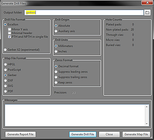
These are my settings when plotting the test design I uploaded:

1 Like

And yes, as @eelik pointed out, removing the .drl file the others look fine:

(sorry for adding so many replies, but can’t attach more than one image per post)

EasyEDA probably has trouble with PostScript drill file, try changing it to gerber.

1 Like

@qu1ck I tried changing drill file to gerber, same result. Howerver, I’ve just tried generating the gerberfiles in another machine, and it works!

It’s really weird, but it seems it must be something with my KiCad installation or with my computer.