Hello,
I’m trying to create a stiffener layer of a flex board in a panel pattern. I finally figured out that zones only follow edge cuts if it’s a copper layer, so I had to add another copper layer to this 2 layer board and use one of the extra layers for the stiffening layer.
Anyway, when I fill the zone, it avoids the edge cut through holes, but it does not avoid the coupon even though I drew lines… it goes inside of the coupon and seems to only avoid the lines…not inside of the coupon.
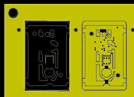
Below, the first picture shows the zone filled …and the second pictures shows the zone before it’s filled. Thank you!
Alex
Can you take a screenshot of just the edge.cuts layer - nothing else?
Also, what net did you choose for the stiffener (copper layer) filled zone?
And, where do you want the stiffener to be and where don’t you want it (= your aim/intention), as I don’t know what your desired outcome looks like.
Thank you for the response!
I didn’t choose a net. The is no net assigned to the zone.
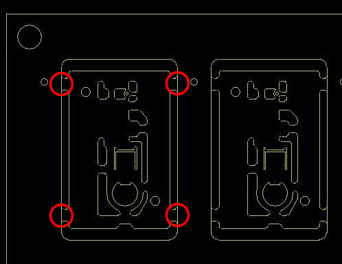
Below is just the edge cuts layer…
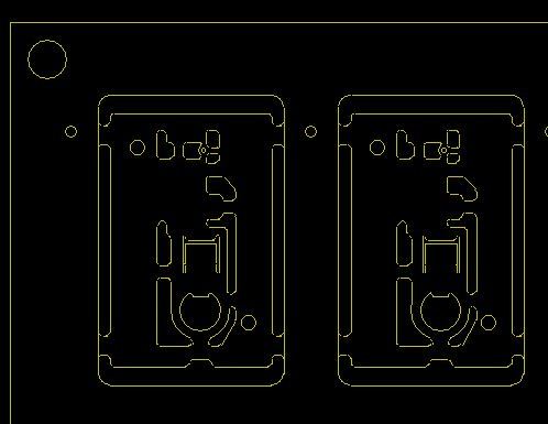
I want a cut out around the circuit board and it’s 4 tabs, except I want it to follow the rounded corners. Below shows the zone with a manual cutout zone, but if I do this, the zone does not follow the rounded corners and I can only create a square cutout. I could add more corners and follow that contour manually, but it is tedious and lacks precision.
I hope that helps… Thank you!
There are (for KiCAD) confusing edge.cuts there.
Do you have confirmation that the stiffening layer contour/area shall be communicated via a filled zone?
Why wouldn’t an outline/contour do - similar to edge.cuts?
you could use one of the Eco layers for this for example - just draw the external outline and the internal cutouts on that layer like you would do for the edge.cuts and you’re done.
From the 2nd image I take it the stiffening essentially is just for the pcb panel - the actual pcb you’re going to use will have no stiffening areas?
Your aim essentially boils down to having a rigid outer frame for handling of the flexible pcbs?
PS: is there a reason those tabs have round corners and the distance between the final pcb and the rigid frame is so large?
PPS:
To actually help you with that zone and your approach:
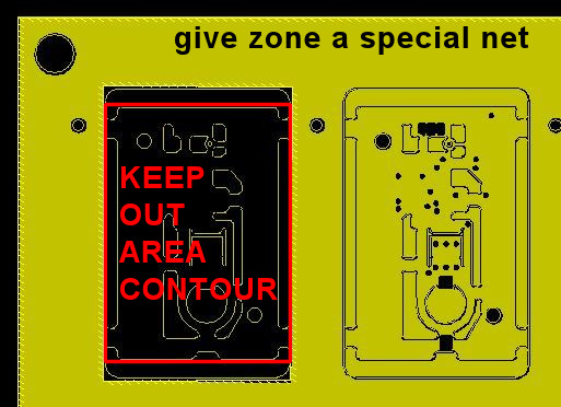
You need to create a special net (net name 'stiffener maybe?  ) in eeschema and some through hole component (as you use an inner layer) that sits on that net for the zone to correctly fill. This component then is placed somewhere on that frame.
You also need to correct the edge.cuts layer and remove those lines on the outside of the tabs - they need to look like on the inside - the keep-out area will take care of it. And you probably have to experiment a little, and check out different states of filled zones and keep-out settings for the gerbers.
If that internal pcb contains any filled zones, you could also use thin keep-out areas just along the tabs (= as wide as them).
The special zone will then only fill those areas where the through hole component ‘floods’ the area. It won’t cross edge cuts and also stop at keep-out areas.
2 Likes
Thank you so much! You hit the nail on the head. I ended up using an outline imported from a DXF onto the Eco1 layer like you suggest. I was using this layer for the zone… I guess I was focusing on the zone fills because I have so many zone fill stiffening regions made with copper in the actual circuit that I thought the FR4 stiffening layer should be made in this way also… This was a great lesson on zones though, so thanks again for your time!


