Hello. This is Xavier.
I’m making a … well, customized PCB. XpandShield_MK2_1.
I’m using KiCad v5.1.9-1.
I had made quite a few boards already. But I never bothered to start from scratch (schmantic, etc) because missing schmantic symbols, such as ones for TP4056, Arduino-Leonardo/AtMega32U4, the SN74AHC1G125DBVR, to name a few. Also in part because my projects involved pre-assembled modules (like the display).
But I can deal with it. Just like how I dealt with the lack of footprints for certain, relatively popular components like the RKJXV ThumbPointer™, the RKJXM Stick Switch, and the Tactile Switches by using non-tented vias (or using generic, modified footprints for SMT parts) acting as thru-hole pads. And I never bothered with the schematic and routed everything by hand.
It worked well, for some time, until I need to create this large project.
And I still managed to route it, quite decently. However, I need to add a Net manually because I need to:
Add a flood fill
Check my manual connections
Check out how will the autorouter route the tracks (potential optimizations of my manual tracks)
And from places such as this and some exploring I found out how to add Net Class. But then I cannot add a Net.
However, on sites like this it was said that it need KiCad version 99 to work.
But you know that we don’t have a version 99.
So, I’m here to ask, “how to do this”?
Just as a general point, even if you shell out loads of cash for a commercial EDA suite, you will still have to design some of your own footprints. It’s generally not that difficult.
I would also encourage you to just draw a schematic. It doesn’t have to be perfectly laid out but it will make working in KiCad a much better experience for you. Whilst you work against the intended workflow you will end up hitting problems. Usually the response is “it’s too simple to waste the time drawing it”, in which case it will take only a few minutes to draw the schematic and head off a pile of issues which are likely to take you longer to work around.
All those big features which may cause instability in normal use are already in. The file format is stable (except for possible bugfixes, but they are few and far between if there will be at all). It’s going more and more stable now in average, not less stable.
5.99 is compiled every day on a number of platforms. It is generally very stable - it is really just in the bug fix stage (a couple of other features are being worked on for inclusion but it is essentially complete) and it should be ready for release hopefully/maybe before the end of the year. It will become 6.0 when deemed ready to be tagged.
It IS not that difficult, however because I had finished the PCB layout (of the components) before I went and made the footprint, I see little reason for me to make them into footprints (especially since they don’t copy-paste into each other).
It take more than a few minute when you are working with defined pins of a unlisted module rather than one that is in the bank.
And even so, I get random “pins not connected” error.
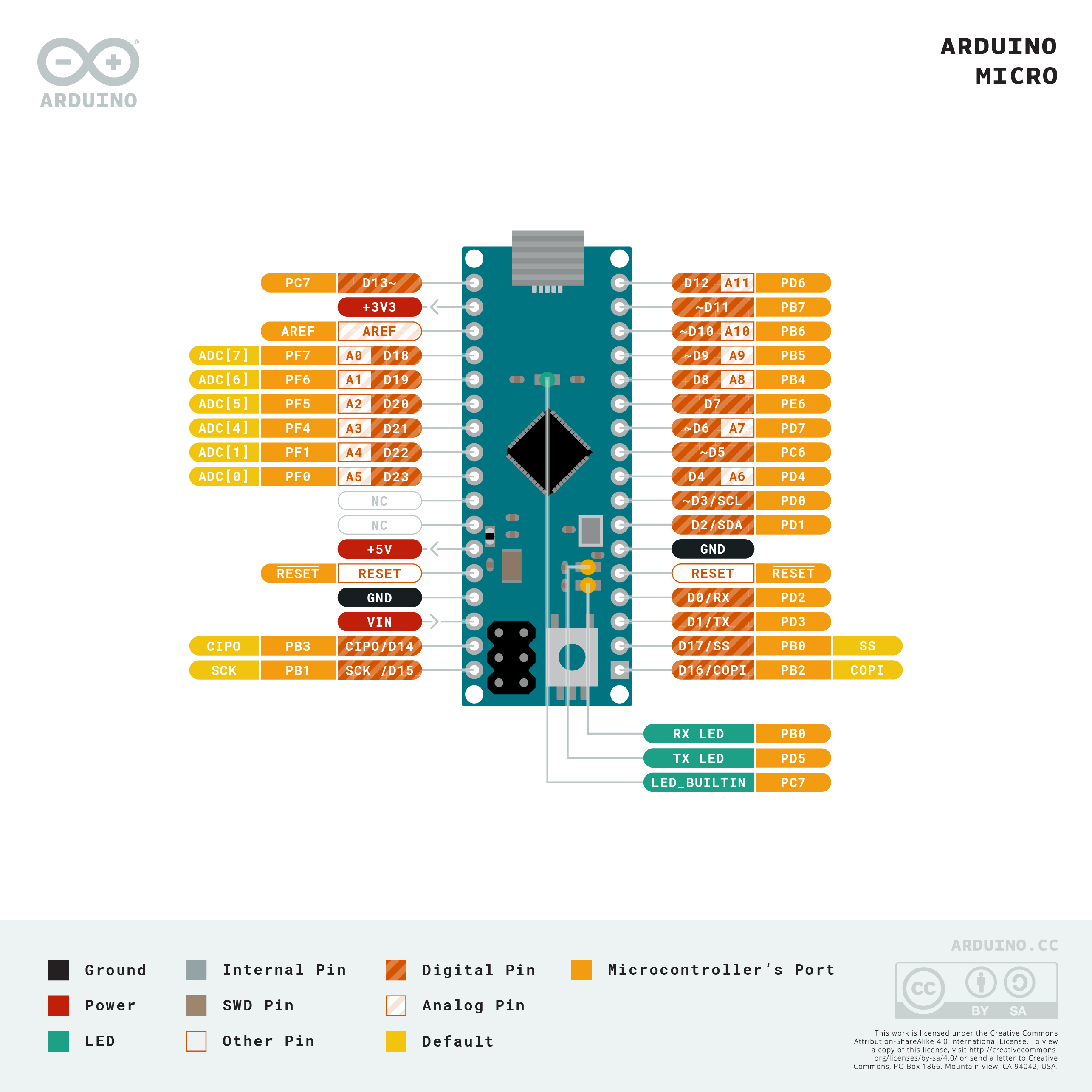
For example, in this simple “potentiometer net” (which is a small part of my overall project), it says that A0, A1, A2, A3, A4 and A5 is not connected to anything, and that “5V pin is connected, but not driven by any pins” which is clearly not true since the A0-A5 are configured as general IO pins (as see on Pinout-Micro_latest.png) and that the “5V” power port is connected to the “5V” pin (and it does not matter which type of label I uses)
Because the problem is that we don’t have a ATMega34U4-XUAU (and it will be crazy to copy over the entire Arduino’s schematic).
Edit:
We have a schematic entry for Arduino Leonardo, however it did not break out the pins on the ICSP header (SCK, MISO, MOSI).
The updated files are on github (post 1)
Can you tell me what number correspond to 5.99 (i.e. “testing 5.1-jenkins-413” or “nightly kicad-msvc.r23444.baf6798695”)?
Your global label 5V is connected to your local label GND (next to P1) and your global GND is connected to the local label 5V near P5. Also you have a global 5V and a 5V power net, and a global GND label but no GND power pin (or flag) Using both local and global labels, the global will trump the local labels but are going to flag errors.
Are your A0…5 labels actually connected and is there another instance of them somewhere where they actually connect to?
It take more than a few minute when you are working with defined pins of a unlisted module rather than one that is in the bank.
But I bet you had a piece of paper in front of you with the pin numbers and functions written down when you routed the board and you will probably want to refer to this piece of paper when you test your board. With this documented in the schematic it will make the whole process easier and less prone to error.
No. They connect directly to the 2nd poles of the 6 Pots.
As mentioned, I am able to locate the “Arduino Leonardo” module and hook up most of the pins I am using, however also as mentioned there is no “ICSP” header (and associated pins) so I will still need to define them myself.
That’s quite helpful. I’ll look into it
You are mostly correct, but I’m not going to
since you copied my number I assume that all of the nightly builds (that are available here) point to some version of 5.99. I’ll pick one at random (and use it).
So next time you need a TP4056 or an Arduino-Leonardo/AtMega32U4 or a SN74AHC1G125DBVR (which you say are all missing from the library) or footprints for your RKJX switches, you are just going to start again from scratch? The time spent drawing them now will be time saved next time you use the same component again.
I did create some footprints. Like the RKJXV and the RKJXM, and the RS**1.
However I did not create schematic “footprints”, for I do not want to bother with it, and for the fact that I do not know how to create one in the first place.
And uh, after some frustration over 0306 resistor arrays, I end up with a working board. Although, lacking a solder fume extractor (or some other things), my throat had not felt too good since.

