Hi there,
I’m very, very new to this software and am trying to get a handle on how to simply modify the edge lines and general layout of an existing file. I’ve spent the last week watching tutorials and for some reason I still don’t know what I’m doing, maybe it’s because I had to learn all of circuit theory in this time (I’m a chemist). Basically, I have a PCB layout with, what seems to be, an associated schematic file. When I try to modify the layout, track lines disappear and everything seems to get messed up. I’ve been told to start fresh and modify the schematic, but there is nothing changing as far as circuitry goes. I NEED HELP 
It’s basically a pogo-pin set up (120 pins, divided into two regions, which corresponds to 60 pads in a rectangular array) connected to three forty pad connector components (I’m really sorry if this doesn’t make sense, but like I said I have no clue what I’m doing).
I can’t help but thinking that there must be an easier way of trying to achieve what I’m doing. Please help.
For a start: Can you post a screenshot of the existing schematic and pcb, maybe with some annotation what you are trying to to? That way we might get a better idea how to help you.
2 Likes
I have four screenshots pending. The firs PCB screenshot shows the complete version that I’m trying to modify, which can be obvious because all of the tracks and vids are present. The second PCB screenshot shows the modified edge cuts and the new placement of footprints. When I move these, the tracks and vias obviously aren’t modified accordingly, so I cleaned up all tracks and vias to make it more clear.
There is a screenshot of the schematic that came with the file, which is supposed to be the schematic for the first PCB screenshot mentioned above. Seeing as though I’ve never worked with this program before, I’m really not sure what to expect. The final screenshot is an error message that I get when I open up a schematic file - I have a feeling that not having these libraries is what is causing my issue, but I can’t be sure. Thank you for your willingness to help.
In your second screenshots there are symbols with question marks. These are the symbols mentioned in the error message. If you want to change anything, you will need these missing symbols.
Normally there should be a file in your project folder called [project name]-cache.lib. This library should contain all used symbols. (Ask the original author for this file)
If you have a file called vheelerlab.lib somewhere, you need to add it to the search path. (If not ask the original author.)
in the schematic editor got to preferences->component libraries.
A dialog opens that can be divided in two parts. (upper and lower)
Use the add button of the lower half to add the directory containing your library to the search path.
After you have done that add the library itself with the upper add button.
In open gl canvas (i don’t know how it is done in legacy, never used it)
Left click on the line. After that the line has white filled rectangles at both ends and a filled circle in the middle.
moving the rectangles changes this end of the line, moving the circle moves the whole line.
To get any use out of this mode you should use a grid that suits your needs.
Another option is to press e while hovering your pointer above the line.
The line properties dialog opens. In it you can enter the start and end coordinates you want.
(The problem is that the coordinate origin is not moveable and is fixed at the leftmost corner of the sheet.)
I always use a 0.5mm grid when creating board outlines. (And use the measurement tool to ensure that i have the correct measurements.)
If you need exact outlines you can use dxf import.
What did you modify?
Normally if a netlist is connected to the layout, missing connections (for example if you delete a track) should be signified by ratsnets. (thin white lines that show you which pad should connect to which other pads.)
Maybe your ratsnets are set to hidden. (Either via the toggle visibility button or in the render tap)
This screenshot is from the opengl canvas. (F11 activates the opengl canvas.)
The ratsnet is quite hard to see in this screenshot.
1 Like
Thank you for your responses - I went through everything that you had advised me to do. The proper library exists in the program now. I’ve played around with this more and I have two more general questions
- I tried to toggle the rat’s nest option on and off in PCBNew (in legacy and in OpenGL) and there seems to be no rat’s nest to display
- The schematic has no connections, I think there is where my main problem now lies. All I want is to have the connections as shown in the layout screenshot with the tracks and vias shown above (the 40x2 connectors connecting to various pogo pins on the sides) - I guess what I’m asking is what would I have to include in the schematic to achieve this?
What would I connect the connectors in the schematic to when all I’m connecting it to are pogo pins?
i.e. If I’m connecting those connector components to 120 pads, would I have to add another custom connector component in the schematic or are the pads represented by another, generic type of component?
Can you post a screenshot of the schematic now that you have the library added?
(I believe there should be connections between the symbols that where once question marks and the symbol that has been there from the beginning.)
Or can you share the project (including the libraries)?
Here is the screenshot of the schematic and what is looks like now. The original files are open source and I can provide the link, but the files on the website I believe aren’t the most recent ones and I do not know if i can share those or not yet, but I will look into it.
Hm it seems the symbols have been changed since the schematic has been originally designed.
(The pin length has changed it seems.)
Hopefully this will help: (Made a fast example of what you have, but with my own symbols so not the same.)
See these 2 red circles within my blue circle? These are the ends of your pins.
They need to be connected.
If you move them apart they are easier to see.
You have two options: connect them while they are apart (use a wire for that)
Or move them such that the ends overlap and the circles vanish:
2 Likes
Thank you! I’ve been looking for the correct component that is associated with a pogo pin, but I’m assuming that this is part of the general library that comes in KiCAD and not part of the special one I’ve added.
I think I would have to add some sort of test point component from KiCAD, which they have in their library.
It seems they used the conn_01x01 symbol for the pogo pin. I don’t now which footprint they used.
(He can check that by pressing E over the symbol and checking what is in the footprint field.)
Thank you, you have helped me a lot. I think I’ve figured it out. I have to add 120 test points individually and connect them the way you showed me above to achieve the PCB layout in the screenshots I originally sent. Thanks to you and @Andy_P I think I’ve finally almost figured this out 
I have one more question regarding wiring. Attached, please see a screenshot of the schematic that I’ve managed to come up with. The issue is regarding wiring. I connected the pins together like in the screenshots you sent, but I don’t think I’m wiring the connectors correctly because I keep getting a wiring error. I’ve put “no connection” on all the separate pins, which seems to rectify the issue, but I’m not sure what the implication of doing this is for the PCB.
Lastly, I’ve attached another screenshot of a footprint I need for the “J1, J2 and J3” components. I can’t find it in the special library that I’ve added to Eeschema. I have the correct footprints for the individual pins, I now just need the footprints for the three groups of 40 pins that I’m using as a 40x2 connector components in the schematic. 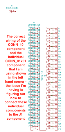
Uploading…
I managed to wire them without obtaining an error while running the bug check. I’m sorry if these posts seem redundant, I’m just getting acquainted with the software. I think this may be the correct way of wiring the schematic. I’m just trying to figure out how to add my .pretty files containing the custom footprints to cvpsbnew. I’ve been looking at other posts you’ve responded to and have been following those steps. It seems like the library seems to add to cvpcbnew, but when I click it on the left hand column no associated files come up on the right hand side for component-footprint association
A few tips to make your schematic more readable:
First off all hide the value field of your single pin connectors.
(press e -> deselect show from the value properties.)
Another thing:
As @Andy_P mentioned its bad practice to have wires crossing symbols. (Makes this makes a schematic incredible hard to read.)
One option would be to arrange the schematic somewhat like this:
This of curse needs a lot more space.
Here a limitation of kicad comes int play. One can not simply have multiple pages (in the same hierarchy.)
Experienced designers can easily work around that but it’s hard for beginners as yourself because you need to learn about this hierarchical stuff quite early on.
First off all try restarting kicad. (it seems some users had problems that libs are not found until they restarted kicad.)
Secondly:
Cvpcb has filter settings. (I hope this image explains it a bit.)
You can also assign footprints without using cvpcb.
Press e while your mouse is above the symbol you want to assign a footprint to.
If you press brows footprints, the following browser opens. (advantage: has a preview of the footprint)
P.S.: yes i made a similar post not long ago to which i could link here, but i can’t find it anymore.


