Througholes not opening up on Gerbers

I sent my board off for manufacture and got a message back saying the footprint holes below are not opening up on the Gerbers. Here is the footprint on my board (The oval thing with the two large TH which are not showing up): -

image

Here is what the PCB house is seeing : -

image
The arrowed holes are not opening up. These are all footprints I did - so they are not from the library.

Here is the ‘E’ window on one of the pads with the detail : -

Here is the schematic ‘E’ window of the part : -

Clearly I am doing something wrong here, can someone point me in the right direction?

Rgds

AndrewR

These coordinates look very suspicious:

image

Pad locations are relative to the footprint origin, From the overall scale of your screenshot, I would expect coordinates smaller then 15mm.

Also, before changing anything, make a backup of your project, including the generated gerber files. This can be valuable if the discrepancy started from a KiCad bug instead of user error.

If you have trouble with further diagnoses, then make a small test project which includes one of your home-brew footprints, and post it here.

I think it’s pad properties from inside the PCB editor not from the Footprint editor.

Did you send Drill files with your Gerbers ?

Just to be clear we are talking about ‘the oval thing’ that looks like a crystal, because in the top drawing the two pads are connected to a blue track ?
:mouse:

Me too. I verified it before posting by looking at the pad properties from a footprint on an existing PCB in the PCB Editor. Those pad properties are also relative to the footprint.

I use a chrome plated paper clip for a test lead clip - so the two holes are indeed connected with a track. The footprint does look like a crystal.

I confirm the E dialog box I pasted up is from the PCB editor, not the footprint editor.

The holes are 8.5mm apart.

I’ll make a quick demo board and post that up. The thing is it looks ok from what I can see on the layout, but the Gerber is not right. I’m assuming when I created the part I did something wrong.

(I noticed I also did not include a courtyard for this part)

Here is the footprint editor dialog box :-1:

I made a quick test board with the test clips I created, and then a part from the library (Wurth THP inductor) as a reference. The Gerber viewer is showing the following

I had to load the THP Gerber drill file as well to get this image. I seems the Gerber reader is saying the holes are there as the orange centre holes are visible on all footprints - but I may be interpreting this incorrectly.

Here is the E dialog box for one of the pads from the library part :-1:

Here is the E diolog box from one of the problematic footprints : -

And this is the E dialog box for one of the pads in the footprint

AndrewR

Any ideas?

I noticed on the library part in the E dialog box for the pad, the F.mask and B.mask layers are turned on (tick in the box) but not on my parts. I edited the pads in the top most test clip and regenerated the Gerbers and this is what I get now before loading the drill file: -

The top test clip looks like the library part so far.

When I add the PTH drill file to the view, this is what I get : -

Now when I add the NPTH drill file this is what I get :-1:

So it seems, the NPTH is overwriting the pad hole information on my creations. How can I fix this properly rather than editing these holes manually?

Thanks

AndrewR

A short while back you wrote:

So where is the project? Zip it up (without the backup directory) and post it in this topic.

rpad_Board.zip (20.9 KB)

I can’t see the project now, I’m with my phone.
The problem is in your 3rd image.
The layers checked for the pad are paste and silk. They must be F.mask and B.mask, that are responsible of the opennings.
Check F.mask and B.mask and uncheck the other four ones. Of course, keep copper on all layers.

Viewing in 3D, most of your pads are covered by soldermask, thus cannot be soldered.

The solution is:

First, you project is in a bit of a mess, and this makes it more difficult to work with it. It also makes it more difficult to judge whether I am looking at the same thing as you are.

I do not know if this is a “beginners thing”, or if you are one of those people who are “inherently sloppy” and not able to apply a bit of structure.

I will start with a listing of the files in your zip archive:

paul@cezanne:~/downloads/rpad_Board$ ls -hl
total 120K
-rw-rw-r-- 1 paul paul   65 Jan 24 19:59 '#auto_saved_files#'
-rw-rw-r-- 1 paul paul 6,7K Jan 24 19:59 '_autosave-rpad board.kicad_sch'
-rw-rw-r-- 1 paul paul 2,5K Jan 24 20:18 'rpad board-B_Cu.gbr'
-rw-rw-r-- 1 paul paul  768 Jan 24 20:18 'rpad board-B_Mask.gbr'
-rw-rw-r-- 1 paul paul  468 Jan 24 20:18 'rpad board-B_Paste.gbr'
-rw-rw-r-- 1 paul paul  469 Jan 24 20:18 'rpad board-B_Silkscreen.gbr'
-rw-rw-r-- 1 paul paul  628 Jan 24 20:18 'rpad board-Edge_Cuts.gbr'
-rw-rw-r-- 1 paul paul 3,0K Jan 24 20:18 'rpad board-F_Cu.gbr'
-rw-rw-r-- 1 paul paul  768 Jan 24 20:18 'rpad board-F_Mask.gbr'
-rw-rw-r-- 1 paul paul  468 Jan 24 20:18 'rpad board-F_Paste.gbr'
-rw-rw-r-- 1 paul paul 7,7K Jan 24 20:18 'rpad board-F_Silkscreen.gbr'
-rw-rw-r-- 1 paul paul 2,8K Jan 24 20:18 'rpad board-job.gbrjob'
-rw-rw-r-- 1 paul paul  22K Jan 24 20:17 'rpad board.kicad_pcb'
-rw-rw-r-- 1 paul paul   48 Jan 24 20:17 '~rpad board.kicad_pcb.lck'
-rw-rw-r-- 1 paul paul 1,2K Jan 24 20:17 'rpad board.kicad_prl'
-rw-rw-r-- 1 paul paul  11K Jan 24 20:17 'rpad board.kicad_pro'
-rw-rw-r-- 1 paul paul  105 Jan 24 19:42 'rpad board.kicad_sch'
-rw-rw-r-- 1 paul paul   48 Jan 24 19:47 '~rpad board.kicad_sch.lck'
-rw-rw-r-- 1 paul paul 3,1K Jan 24 19:51 'rpad board.net'
-rw-rw-r-- 1 paul paul  285 Jan 24 20:19 'rpad board-NPTH.drl'
-rw-rw-r-- 1 paul paul  615 Jan 24 20:19 'rpad board-PTH.drl'

The gerber files (and drill files) obfuscate the rest of the listing. I prefer to put them in a sub directory. That cleans it up a bit:

paul@cezanne:~/downloads/rpad_Board$ mkdir gerber
paul@cezanne:~/downloads/rpad_Board$ mv *.gbr* gerber/
paul@cezanne:~/downloads/rpad_Board$ mv *.drl gerber/
paul@cezanne:~/downloads/rpad_Board$ ls -hl
total 76K
-rw-rw-r-- 1 paul paul   65 Jan 24 19:59 '#auto_saved_files#'
-rw-rw-r-- 1 paul paul 6,7K Jan 24 19:59 '_autosave-rpad board.kicad_sch'
drwxrwxr-x 2 paul paul 4,0K Jan 24 21:51  gerber
-rw-rw-r-- 1 paul paul  22K Jan 24 20:17 'rpad board.kicad_pcb'
-rw-rw-r-- 1 paul paul   48 Jan 24 20:17 '~rpad board.kicad_pcb.lck'
-rw-rw-r-- 1 paul paul 1,2K Jan 24 20:17 'rpad board.kicad_prl'
-rw-rw-r-- 1 paul paul  11K Jan 24 20:17 'rpad board.kicad_pro'
-rw-rw-r-- 1 paul paul  105 Jan 24 19:42 'rpad board.kicad_sch'
-rw-rw-r-- 1 paul paul   48 Jan 24 19:47 '~rpad board.kicad_sch.lck'
-rw-rw-r-- 1 paul paul 3,1K Jan 24 19:51 'rpad board.net'

Note that you can type in a directory name in KiCad itself when you generate gerber files.

rpad board.net I don’t know why you created this file. Netlist files have not been used for normal operations for 5 years or so.

Next problem, there are two lock files, the schematic file itself is just 105B in size. There is an _autosave-rpad board.kicad_sch with a file size of 7.6kB though. An attempt to open the project, open the schematic and restore does not work. I get this message:
image

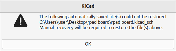
Weird. After exiting KiCad the “_autosave…” file is also gone.


Delete & restart.
I deleted the old schematic, renamed the _autosave-rpad board.kicad_sch to the normal schematic name and deleted the lock files, and the netlist file.
Project now looks like:

paul@cezanne:~/downloads/rpad_Board$ ls -hl
total 56K
drwxrwxr-x 2 paul paul 4,0K Jan 24 22:03  gerber
-rw-rw-r-- 1 paul paul  22K Jan 24 20:17 'rpad board.kicad_pcb'
-rw-rw-r-- 1 paul paul 1,2K Jan 24 20:17 'rpad board.kicad_prl'
-rw-rw-r-- 1 paul paul  11K Jan 24 20:17 'rpad board.kicad_pro'
-rw-rw-r-- 1 paul paul 6,7K Jan 24 19:59 'rpad board.kicad_sch'

It also opens normally. both schematic and PCB are visible in KiCad’s editors.
In the 3D viewer, it looks pretty much the same as what dsa-t posted.

Opening footprint TP2 in the footprint editor.
One pad is at (0, 0) which is good, the other is at ( -0.071165, 8.372621) which is odd. You make it easier for yourself if you put all pads on a reasonable grid.


Opening TP4 in the footprint editor, I see similar, but different coordinates. Pad No.2 is now on (-0.064347, 7.142608) All these footprints also have lines on copper layers. That is not good.

I also see that you have no custom footprint library. The schematic links to two different, but non existent footprint libraries too. The schematic symbols do have real pins with pin numbers (but hidden) That is … acceptable.


All these problems are not so difficult to fix if you know what you’re doing. You are obviously a beginner with KiCad. Maybe you have more experience then I would estimate form this test project. Your real project may be in better shape.


Another cup of tea…

Fantastic Thank you!

During my cup of tea I’ve been looking at your gerber files. The main problem with those is the fault in the solder mask as already mentioned.

No it is not. There are no drill locations defined in the NPTH file.

Are you familiar with library management?

The best way to proceed is:

  1. Create a project specific symbol and footprint library.
  2. Put your symbol and footprint in it.
  3. Fix the library footprint.
  4. Make sure to update the links in the schematic, so all use the proper footprint.
  5. Update the PCB, this should also put updated and fixed footprints on the PCB.

Do you need help with those steps?

I started with KiCAD 10 days ago, so I’m afraid I’m on a steep learning curve.

When I started with KiCad (KiCad V3 or V4) the “Getting started with KiCad” guide was really good. I made my fist test project with help of that guide in the first afternoon. But then it did not get updated for several years, and it dot behind a lot.

I am not sure how good the current “Getting started in KiCad” guide is. It’s now over 7 years ago I started with KiCad.

To ease your learning curve, try to bite of smaller pieces. It’s quite common for beginners to make a bit of a mess of things. Because they don’t know (yet) very well what they are doing they do some “weird things” and they also do not know how to fix it later. But be patient and give it some time and effort and you will improve.

1 Like

I came in at the end of V4 and that was tough for me I had never used any EDA software at all and I still had Ferric Chloride stains on my hands I found following basic YouTube videos for a few weeks help a lot and also the Kicad Doc’s are so much better now. Personally I get my schematic finished before I even think of a PCB and Gerber files. A finished schematic with no ECR problems then its off to PCB editor. What I am trying to say maybe slow down a bit and get the basics nailed, maybe ?
:mouse:

1 Like

Thanks for that. Is there any way to put the own footprint library where it can be accessed by all projects, or do I need to copy my personal library into each project file?

How do you create a footprint and symbol library?

AndrewR