I am trying to tune the length of a trace with a very “tight” pattern.
It seems that it is not possible to have the space lower than ~0.2mm. At a certain stage the pattern stays the same, no matter how low I put the “min spacing” value.
Is there a minimum allowed value for the minimum spacing? is it hard coded or configurable (where?)
By editing the tuning parameters of a “rectangular tuning block” and setting it to single sided, you can halve the amplitude of the squiggles.
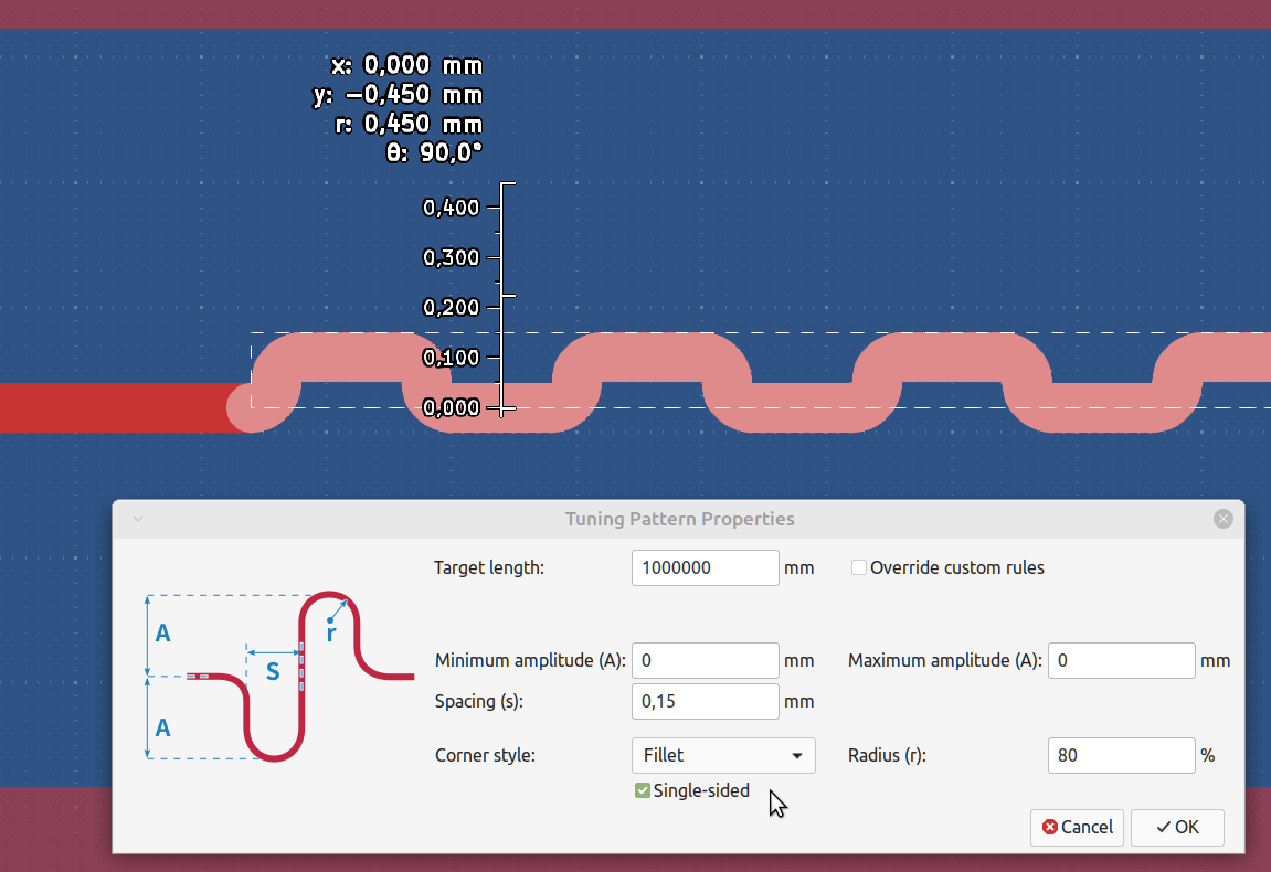
Th track width also has a significant influence. Apparently the (single) amplitude of a squiggle has a limit of the track width, and by reducing track width to 0.01mm, I can also make the amplitude of the squiggles smaller.

Can I ask why you need such tight length tolerances?
Assuming that the transmission speed in copper is 15cm/ns, you’re looking at sub picosecond delays for each 0.2mm difference. There are very few applications where this level of precision is required.
I am implementing a heating unit on a flex substrate. I need to put a certain resistance ino a certain area. Laying it by hand will be tedious and i thoght that the track length tuning would make the work much easier, which indeed it is, but limits the space (and reducing track width did not help in my case - I am not trying to reduce the size of the wiggle, but the space between the two vertical paralel tracks)
I’ve never implemented an ohmic heater on a PCB/Flex, but I would think that you would want long straight tracks of a specific width to get the desired resistance. Having the jagged pattern of the line length tool probably won’t be as space efficient.
What is your definition of “tedious”? Sometimes you just have to risk carpel tunnel syndrome running a mouse back and forth.
Don’t forget that you can cut and paste track segments in KiCAD.
Don’t think I’m discouraging such a fine-dimensional design, if you really need it and are willing to pay($) for it but, who is going to make it? And, what’s the cost and Quality Control expectation?
Check out the thickness of an average Human Hair…
Amongst my many (real, world product) designs and oversight/mgmt of other’s work, my work included Catheters for Human Hearts and Ophthalmic tools (and Chips for Intel), it was 25yrs ago so, I don’t know what micro-technology production costs are in today’s world but, I doubt this is low-cost…
That said, and tweaking tuning parameters, screenshot below shows Resistance for a Straight Track and squiggled Tuned Track…
Placing two tracks with 0.2mm distance/gap is about Dragging one track close to the other with Kicad’s Grid-snapping disabled.

I did not fuss/bother with Gap’s between squiggles and straight track

And, each Segment(s) of the Track can be dragged to accommodate your geometry needs… Dragged several segments below… Naturally, you can delete some and tweak the remaining one’s to close gaps…etc, as needed…

It is limited by track width and your clearance values.
If you reduce clearances, make sure that you’re within PCB manufacturer’s specifications.
1 Like
In v8+, you have to “Ungroup” the tuning pattern before you can edit individual segments/arcs.
It would have helped if you mentioned that in the beginning.
As dsa-t already mentioned, the maximum frequency of the wiggles is defined by the track width + the clearance.By setting both the track width and the clearance to a small value you can reduce the geometry.

Also, maybe you find the “KiMesh” plugin useful. It’s original intention is for a “security mesh”, and it adds funny looking patterns to your PCB. Much better then the boring squiggles ![]()
Board setup has no space or track limits (boxes are empty so I guess no limit unless there is a default for no value).
track width went down to 0.1mm with no problem but space refuses to go below 0.2

Thanks,
Not next to my design now, but probably this is where my limit comes from.
I was looking only someplace else for this limit (maybe at the constraints screen).
Flex PCB manufacturers do not seem to have a problem with 0.1-0.15 mm at standard production.
True for some vendors but, perhaps not all.
Now, the important part (maybe…)
I did Not prepare my geometry before making the video below (too lazy) but, you’ll get the idea… Edit a section, Copy and delete the middle segment (the one resulting from the 0.2mm min Space setting), paste the segment and tweak it’s length then, put together a complete unit. Note: this has a ‘One Sided’ setting so, all the sections are above the centerline of what would normally be a =/- amplitude…
Then, make an Array as long as you want it… Thus, spacing is now less than the minimum setting…
Why all this weird twiddling with segments when you can simple drag the “length tuning box” to any size you want?
What’s the smallest spacing? (I suppose I could/should try it but too lazy and I don’t have v8 installed…)
EDIT: I missed it in your post but, now Got it, needed to set the Clearance in the NetClass, too. Thanks, @paulvdh
1 Like
Yes - this solved the problem.
indeed I looked in the constraints screen and not in the net classes screen
Thanks again
1 Like
This topic was automatically closed 90 days after the last reply. New replies are no longer allowed.