I have 105 switches (keyboard) individually connected to GPIOs, which is why I also have seven I/O expanders that also have five connections to MCU each. So, lots of traces.
It doesn’t really matter which GPIO pin each switch is connected because firmware is going to figure out those details. I would like to have some freedom when drawing up all those traces and decide in PCB designer to which chip draw traces from which switch instead of strictly following schematic editors plan.
I understand that those restrictions are there for a reason and I’m not complaining, I’m just asking if there’s a good way to archive what I want to do because in real world and in this case those restrictions are too restrictive and those connections should be allowed to be made the best way possible.
I’m a newbie, so it’s more than possible that I have missed something. If that’s the case, please tell me.
This is a variation of “pin swapping”, a long requested feature
1 Like
Okey, thanks! So, I probably have to just cope with swapping switch footprints with Alt+S then when needed, unless I can figure out some more clever way to do this.
My usual method for this is to first draw the schematic and don’t worry about it. And later when you are drawing the PCB, you change some labels in the schematic manually and update the PCB.
A few other hints:
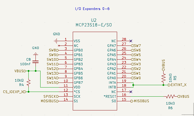
Do not use the Earth symbol for GND, but use the GND symbol instead. Using the earth symbol is confusing as it implies a specific usage.
With MOSIBUS, MISOBUS and SPISCK you’re being inconsistent in naming signal wires that belong to the same group.
There is the WireIt plugin that does pin-swapping and other things. It supported up to KiCad 7, so it may still work.
Yes, there seemed to be many of those swapping plugins and I already made my own version too. 
swap-nets.py.txt (1.8 KB)
