I just made a little mini tutial on how I would use array and block functions to create copies of features in a repetitive design. By using copies and arrays a lot of tracks can be layed out quite fast this way if your schematic / PCB structure is suitable for it.
For other, more advanced ways, scripts such as the “replicate layout” script are much more suitable.
Using arrays and block moves is very intuitive and easy to learn and it seems a worthwhile technique to have in your toolbox.
Making this mini tutorial also made me look differently at Pcbnew. Instead of just placing components and routing tracks I looked at it from a more drawing oriented point of view. Finding common features, and making as much use of blocks and arrays as practial.
Making the tutorial was fun to do and took almost 3 hours out of my life, I hope it’s usefull to somebody.
I’ll replicate my experiment. Let’s see how long it takes (Including screenshots).
13:06 Started “eeprom project” and added a 27128

13:09 Add a wire:

13:10 Clone the wire with the [Insert] key:

13:11 Draw label “A0”

13:12 Replicate the label with [Insert] key. (Label auto increments !!!)

13:14 Repeat for databus:

13:15 Copy once, paste trice to make for of them:

13:17 Copy all for and paste to make 8 of them.
13:18 Annotate + [F8]
13:20 Look at that beautifull ratsnest:

13:22 Placed the 8 DIP’s on a 100mil grid.
13:25 Drew a trace consisting of 5 segments:

13:27 [RMB] / Select / Filter selectrion

13:29 Drag your 5 segments to some empty area:

13:34 Pcbnew / Inspect / Measure (Phew, difficult screenshot to keep it small).

13:37 [RMB] / Create Array (You can enter “800mil”, Kicad will translate to 0.8in.

13:40 We’ve now got a bunch of squiggly traces. All are from net “A6” (ratsnest!).
13:44 Copy the array and paste it over your components:

13:46 Note that more ratsnest lines have appeared.
When zoomed in you see that the traces now belong to different nets:

13:50 Because I made a copy of the original array, I can easily make another copy for the other 4 eeprom IC’s:

13:53 I drew another section of 5 trace segments for the odd pins:
I did these on the other layer for visual impact.
Board sections like this are usually routed with horizontal traces on one side, and vertical traces on another side.

14:02 I’ve temporarily turned the Top copper layer off to easily select the green trace:

14:04 [RMB] / Create Array (in situ this time) with the same array parameters as the red.

14:14 Experiment. Let’s try something new. I deleted U5, U6, U7, U8 & traces:

Idea is to replicate Layout traces and components.
First make the Green stuff Red, we do this with:
Pcbnew / Edit / Move and Swap Layers

14:18 All traces are Red again, I also made a copy and placed it on the former place of U5 … U8.

14:24 Hovered the mouse cursor over the copy of U1 and changed it’s reference to U5 This changes both the text on the silk screen (Above the IC) and on the Fabrication layer (Center of IC).

14:22 Time for a quick DRC check: Pcbnew / Inspect / Design Rules Checker.

14:33 I’ve hidden the copper to make the errors more clear. U1 Through U4 have some errors, but that was to be expected. Those errors are on pins which are neither Data nor Address lines, and we did not bother to connect the rest in the schematic for this mini tutorial.
On U5 through U8 all the pads with copper have DRC errors though.
This is the first time I have to use my brain in this tutorial (oops).
14:37 I’ll post it now, and edit later.
14:40 That was quick / Easy. When I deleted U4 … U8 the connections for those were also removed from the netlist. Going back to the schematic and [F8] corrected that.
14:44 What’s left is a very limited number of DRC errors on the pins that were not connected in the schematic. You can remove these by hand, or use:
Pcbnew / Edit / Cleanup Tracks and Via’s

14:46 That nicely cleaned up all tracks where they do not belong. time again for a quick DRC. No DRC violations, but still 22 unconnected.
14:53 Let’s try to be smart. Were experimenting with arrays and duplication here.
14:57 With the ruler / calliper we measure the distance between the rows as 1700mil.
14:58 Let’s do crasy and see what happens.
15:00 Just drew a green verticl trace 1700 high and vias on both ends.
15:01 I drew a bit too much:
15:03 Wen you want to delete such a segment, the default is to delete the track upto the last pad or split from another track. There are multiple ways to influence this behaviour, but as we’re pretty much freehand drawing we simply turn it of with unchecking the checkbox in:
Pcbnew / Preferences / General Settings / Legacy Routing Options / [ ] Auto-delete old tracks.
15:11 I just drew myself a nice array of “jumper tracks” with these settings:
I do not know what the “Stagger” thing is, but it’s apparently not important now.
15:13 The result of my (much to big) array looks like:
15:16 I set my grid to 50mil, grabbed a bunch of those “Jumper tracks” and dragged them to a new destination:
15:26 I selected some more blocks of the “jumper tracks” and dragged them to somewhat random locations to make connections. In the meanwhile I had
Pcbnew / Inspect / Design Rule Checker


open, and did checks for open connections. Just kept on repeating untill everything was connected. The intermediate result now looks like:
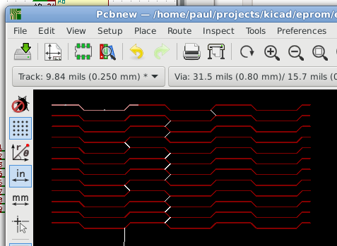
15:31 On the right is still a bunch of left over jumper traces, and also between the Eproms there are some jumper tracks that do not line up. These get easily all get cleaned up with:
Pcbnew / Edit / Cleanup Tracks and Vias.
15:39 As a last step we inspect the result further with for exmple “Highlight traces”. You can see that at least one of the jumper traces made a loop.

In a real world design all those memory chips also have to be connected to some microprocessor or bus GND & VCC nets, chip enables etc. have to be routed. But that is not the goal of this mini tutorial.
Deleting U5 … U8 and renaming the copies was an experiment and it worked quite good. Alternatively you can of course only copy the traces, or copy everything and delete the copied components and then place the orignal components on the positions the copies were.
A very convenient way to place lots of components by hand is to have the schematic open to look up part numbers, and then in Pcbnew use the shortcut “T”, followed by the RefDes of the component you want place. This avoids the need to zoom out / search / zoom back in again and just attaches the component you want to your cursor.
15:50 That’s it for now. Have fun.
Of these almost 3 hours, much time went into figurering out how to do things, making screenshots and writing the text. Without that overhead the example could be done in a few minutes.