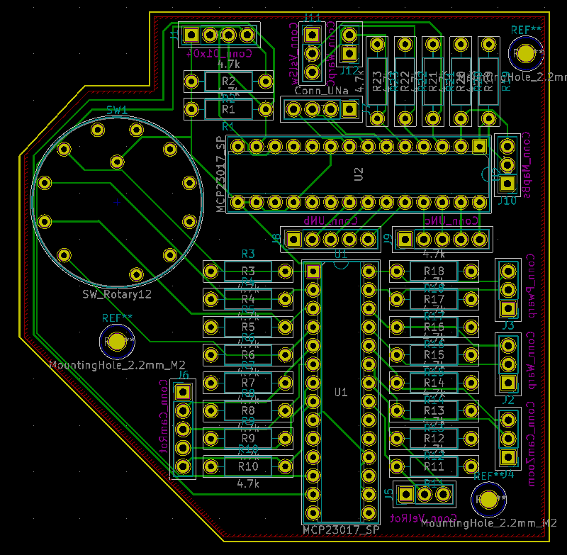
So I’ve seen lots of posts about design rules for various boardhouses, and I designed a layout that I think (famous last words) would work just about anywhere:
BUT after looking at prices for a prototype vs at my university makerspace, I’m likely going to be making something myself on 2 layer FR2. They are pretty anti-chemicals, so I’m not sure I’ll even be able to use a solder mask. I’m guessing I’m not going to be able to solder something that doesn’t short things out. On the plus side, I only need 1 for now, so I can take the time to tweak things if need be.
Anything I can do in layout to make this easier on myself? I’ve got all the traces on the back and a ground plane on front. All the components are through hole, and go through the front except for the headers, which I’ll need to mount on the reverse of the board for access.
Chemicals are one thing but more important is how do you put etch resistant stuff on the board. Photoresistive method, direct toner transfer, something else? Anyway, about the best you can do with commonly available printers and very steady hands is 6-8 mil traces and 6-8 mil clearance. This board obviously doesn’t require that, just as a ballpark, this is the limit past which doing things homemade is just getting stupidly expensive.
General advice for any home made board is to keep both minimum trace width and minimum clearance as large as possible. Minimizes risk of trace continuity and shorts issues. Makes hole/via alignment easier too.
Looking at your pcb you easily could make all traces twice the size and space things out a bit to avoid tight spots with small clearances.
What process are you thinking about using for making the board? The etching is usually the cause of grief over avoiding ‘chemicals’ - are you planning to mill the board on a router? If you are going to use any sort of home process, you are unlikely to be able to get traces reliably down to what looks like around 5mil in your design; probably looking at 10 to 20mil minima if you are making the board yourself.
I stopped making boards when I realised that I could get this shipped from one of the Chinese board houses for £10 or less - and not much more for an smd stencil. I am surprised the economics work for you - I struggled to even buy FR4 for less than the Chinese fabs were making boards for.
About 1990 I used technic: IC - through hole, R,C - SMD 1206.
Just consider it - PCB would be simpler. Don’t wory about assembling SMD by hand. I’m not young, but see no problem in 0603 assembling.
The professional PCB is much better then home made. I have heared people order them in China for really small prices. But I have never did it as we have here (Poland) the good PCB producer. They have the special offer for prototype. Normally it is really more expensive than China, but typically once per month they have a promotion day (last was 10.01) - for 2 layer PCB you pay about $4 + $5 x PCB size (dm). So 10x10cm PCB that day is about $9. But 5x5cm is about $5.25. I think their business is that if they collect many orders one day they can do it chipper as they need not to put into process forms with too few small PCBs on it. It is probably still more expensive than China but not too much.
China probably has such situation day after day without any promotions needed to get many orders.
I have written it just to say - look around - may be you have access to something like that or consider China. I can’t point exactly where to order in China as I have never did it.
Added a little later: Of course IC on top, 1206 on bottom.
There is no way to make your own through holes. Alternatives like rivets don’t work well, suffering from long term corrosion. (Look up about Quad 34 preamplifier board trouble)
Just go to China. Making your own boards makes zero sense in 2019.
JLCPCB will give you 10 beautiful boards with solder mask and silkscreen for $2.00, and with $20 DHL shipping you’ll have them fabbed and delivered in under a week.
I would agree with the comments on China. I am a noob with KiCad but used to design circuit boards for decades before I retired, and the prices I used to have to pay for prototypes “back in the day” was obscene compared to the 2 dollar JLCPCB deal nowadays. Usually home made, means time is not a factor so you can select the “slow and cheap” shipping option too. I’m planning to use JLC for the first time in a few weeks. Once I am a bit further up the learning curve with KIcad, but I did a test generation of some Gerbers the other day and uploaded them to JLCPCB and “poof” there were the images on the screen, and everything looked perfect. Then I realized that I could panelize the boards myself to max out the 10x10cm and suddenly I had 150 PCBs on 10 panels for - yep - 2 bucks plus about 10 dollars shipping to Canada. I spend more than that on lunch every day - LOL
Now if the Canadian government would stop tossing Huawai executives in jail, and the Chinese would stop tossing Canadians in jail, this fantastic new approach to DIY PCB design might continue for me…
@mrpeverill Another reference you may be interested in is:
This site will allow you to get fairly accurate (no quoting process is completely accurate, especially 3rd party quoting services like this one) quotes for boards including estimated shipping costs to where you are (by country). JLCPCB may well be the (or one of the) cheaper options, but this site will help you determine if they really are. (A more local board house might have slightly higher board prices, but for your quantity lower shipping cost might more than make up for it.)
When choosing a board manufacturer, don’t forget to verify their manufacturing minimums (trace width, copper spacing, copper to board edge clearance, minimum drill sizes, etc) against what you designed. Rule of thumb is to not try to meet the vendor’s minimums exactly, but design to slightly larger than minimums so plus/minus tolerances don’t bite you in the sits-upon.
The makerspace offers double sided fr2 in small sheets for about $3. FR4 is more expensive ($12) but I can’t think why I’d need it.
They have an LPKF Protomat plotter that I can use to actually cut the board.
I haven’t looked in to the Chinese fabs much and I should. I know the quality is good enough for this. I’m hesitant because of shipping (My first board may not work) and because I actually have a fair bit of surface area because of mechanical concerns and my use of DIP and through hole components.
Seriously, check out PCBShopper to see what the estimated shipping will be from several different vendors. You enter your board size based on the containing bounding box. (so, yes you are still paying based on board area you aren’t using, but that is how they are usually laid out for manufacture by the automated systems.) No one seems to charge per drill hit anymore. 5 minutes of your time to see if it is really worth it to try to spend hours manually fabbing the boards.
For home made pcb y prefer to always use ticker traces, between 0,5 and 1 mm for low current signals, the ones on your design look thinner than necessary. Also increase the width of the annular rings (to avoid destroying the pad if you drill by hand) and clearances.
I’ve been able to etch pcbs at home that contain an LGA-12 package and 0.25 mm traces but it is very difficult.
I think if you just made the board outline square or rectangle, that would reduce your cost for prototype boards even here in the US and make them more economical. All you’d need is a carbide blade of some kind to trim the angles you want. I’ve used carbide embedded jig saw blades, circular saw blades, and bandsaw blades. Put silk lines on the board so you know where to cut. So you’d be doing some of the work yourself and the board house wouldn’t have to charge you for the labor (even though it’s machine made). They still charge extra for extra cuts past the square or rectangle because of board waste. The other trick is to make the board outline a mirror image somehow and step and repeat it to a standard sheet size (check with the board house). That’s sort of fun fignuring out how to make the board so it’s mirror image can be made opposite and create no waste between the boards. So there’s no, or minimal waste when all the boards are cut out.
These days, I’d sure have a board house in the US make a few prototypes rather than China…one word…Customs. Sometimes WEEKS before they decide your item is OK to ship on. Meanwhile you’ve paid already, deadline is approaching, and you have NO RECOURSE to get your money back.
There are US board manufacturers who do prototype service. No, they aren’t as dirt cheap as some of the China fabs, but there is the benefit of not being on the other side of customs, and less of a language communications barrier for design questions and issues.
Looking at PCBShopper, I see BasicPCB, Bay Area Circuits, Advanced Circuits, Accutrace PCB4U, OSHPark, and ExpressPCB. There are even a couple Canadian outfits there (might be easier on Customs, I’m not sure how the revised NAFTA applies). I’m sure there are even more than what is listed on PCBShopper, let your fingers do the walking.
Once I have done the square prototype where circular PCB was internally defined by mill (from dictionary not sure) with only few bridges left. So I had only simple cut it and few moves of file (also from dictionary).
Ok if I order from JLCPCB, I can get all my designs printed for like 6 dollars (provided I am willing to cut them out myself). It does seem, at that price, that it doesn’t make sense to fab myself (since even with the plotter I have access to I’ll be restricted to using FR2 with no solder mask). Currently my plan is to order the parts with a silk screen divider between boards, and then see if I can cut the finished board using the router in the plotter or a mill of some kind (but the makerspace may not be willing to let me do that since it will already have the solderscreen on there). If not a carbide blade should do it.
I wish the US shops were more economical, but it seems like $50 is the best they could do. Maybe they make more sense at high volume? I think it’s a shame that I have to pay so much more for panelization, in particular, since I think it saves materials over-all.
Generally I use OSH Park (in the US) for small boards, because they are $5 per square inch with free shipping. For larger boards, I use JLCPCB or Elecrow (in China).
For what it’s worth, I’ve never had a problem with customs when using the DHL shipping from China.
How big are your boards? In my experience, if they are less than 10cm x 10 cm, Elecrow (and probably others) will edge mill to shape at the cheap rate - and if the board is significantly smaller, they will panellise it for you so you often get several more boards than you were expecting.