Yes, it is true. I will modify that, thank you.
bitmap2component
but you cannot assign a net to a fp poly zone, so I suggested to create a FZ from those poly shapes
a nice solution would need a code modification as Marco Hess suggested
https://lists.launchpad.net/kicad-developers/msg18709.html
but this is not an easy path because it involves code reworking-testing
a useful workaround would be to have a tool to convert DXF in a multiple pads module, so it would be easier to have RF parts as footprint
may be @Joan_Sparky could think something about it


I had a short stroll on google though…
- http://mathoverflow.net/questions/28303/split-polygon-into-minimum-amount-of-rectangles-and-triangles/28350#28350
- http://mathoverflow.net/questions/80665/how-to-cover-a-set-in-a-grid-with-as-few-rectangles-as-possible
- http://stackoverflow.com/questions/5876188/filling-a-rectilinear-polygon-with-rectangles
- http://stackoverflow.com/questions/20220215/minimum-number-of-rectangles-in-shape-made-from-rectangles
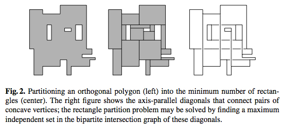
Graphically they all talk about something like this (with/without holes makes a difference and also what kind of specifications the rectangles need to have)…
If I find some free time I might actually try this, but don’t hold your breath please.
No really, don’t hold your breath.
I implemented the idea of substituting polygons by as much rectangular pads as needed to cover the same area. I gave them the number 3 and added a pin on its schematic symbol. Then, I connected pin 3 to GND and regenerated the netlist file.
Here, the footprint:

And here, the result on the layout:

I can say it is a progress however I lost the non-copper zone in the middle part. I don’t know how to avoid the fill in this area.
Hm… quick-fix - place a no-fill zone in the size of the footprint (roughly where the vias are) on the pcb?
I don’t think you will be able to ‘transplant’ something like this into the footprint unfortunately:
(zone (net 0) (net_name “”) (layer F.Cu) (tstamp 5697C758) (hatch edge 0.508)
(connect_pads (clearance 0.3))
(min_thickness 0.2)
(keepout (tracks allowed) (vias allowed) (copperpour not_allowed))
(fill (arc_segments 16) (thermal_gap 0.508) (thermal_bridge_width 0.508))
(polygon
(pts
(xy 126 94.2) (xy 126 98.4) (xy 128 98.4) (xy 128 94.2)
)
)
)
EDIT: NOT WORKING…
One idea… probably not working, but you can try…
Create a SMD pad, same/similar size as the zone I suggested in the footprint above.
Change it’s layer to something like Cmts.User only.
Maybe it keeps the fill out - fingers crossed.
The more practical and useful solution that I got was using keep out zones. It works but I need to define the keep out zone on the layout. So, whenever I move the footprint I also need to do the same with the keep out. Ok, it’s not so complicated but it’s just a workaround, not a final solution.
Anyway, thanks for your help.
Here, the final result:

1 Like
Currently interested in some of this myself. I find it strange you can draw polygons but not assign them to the copper layer in KiCAD footprint editor?
I suppose this should be an easy fix in the code? No?
RF question: Why CPW for input and ouput and not microstrip? Because of FR4 & 2 layer board?
Not worried about transition from CPW to microstrip filter and back to CPW? (Guess would depend on frequency)
You can’t draw filled polygons in the fp editor currently, that’s why I asked up there where those came from.
And even if you get them done via Bitmap2Component module (start via KiCAD main menu), they won’t attach to any net, thus you can’t flow or use them really (unless you disable DRC).
One thing is for sure, those DEFs as footprints need a way to draw filled polygons (even with arc outlines) and a way to specifiy no-fill areas. All possible in PCBnew on board level, but not in the FP editor - on footprint level.
IMHO the fp editor needs an overhaul and more options. Dunno when this will happen though as they just went over that part of KiCAD and now focus on EEschema afaik.
1 Like
@Joan_Sparky
if they would add just the ability to add filled poly to a net would solve the pcb issue… (using Bitmap2Component for designing the poly)…
I had asked some RF improvements a month ago
https://lists.launchpad.net/kicad-developers/msg21602.html
but unfortunately, as you pointed out, they are focusing on eeschema…
@tipofthesword
I’d like to start playing a bit with RF/high speed signals, but I’m really a newbie in that field…
would you mind to suggest me where I could get some tips to start working with?
I mean I found some tech advice at
https://www.maximintegrated.com/en/app-notes/index.mvp/id/5100
but I was wondering if there is some video/doc about some simple RF circuit design with basic examples, or some nice book…
Hey, @tipofthesword
Nice questions!
Actually it’s possible to assign polygons to copper, you just need to edit the kicad_mod file, that’s easy.
In this project I used CPWG because it’s possible to isolate the signal and avoid interference applying stitching vias. Additionally, you can reach the same impedance using CPW with a narrower transmission line width than using microstrip lines, almost two times in this case. This is also important since I have to connect the tracks in tiny smd pads.
The transition between CPW and microstrip is a “critical” point because there are differences between the propagation modes of the structures. However, I simulated the filter model in an EM software and everything was OK. I also built a prototype and everything works just fine. The frequency in this case is 2.4 GHz.
Good point about the filled polygon. Hadn’t realized that…
I guess I’ll also have to go the bitmap2component route and then edit
manually in PCBnew.
By the way, the PCB board is not complete in the last figure. Every track will be surrounded by stitching vias, not only the filter structure. I doing this part right now and I can point out another good RF feature which would be very good to have in this case: a script to automatic add those stitching vias around the tracks where RF signals are flowing.
Unfortunately, I have almost zero experience with python and I’ve never developed any script for kicad.
+1
and here are your 20+ characters, you /piiep/ forum
@viniciuslbar
have a look here
https://lists.launchpad.net/kicad-developers/msg19528.html

and here
https://lists.launchpad.net/kicad-developers/msg21865.html
you may need to build your version of kicad, but may be you can get some useful tools
and here some tips to do stitching vias with the stable release
1 Like
That looks neeeaaaaaat. Thx for sharing.
NEAT
P.S: Do I just need to download the version and compile it? Is there a how-to of the feature somewhere?
yes, but I don’t know why there are 4 repos, one for via stitching, one for via shielding, one for round trace and one for net solder clearance …
I’m going to contact Ben and I’ll be back
Looks amazing!
Depends on the frequency of intest. If you’re interested in general RF work.
That means HF bands to 30 MHz, low VHF/UHF (~150 MHz to 800 MHz for UHF) I can recommend:
It is a very detailed book with nice examples and not too heavy on the theory. It will introduce you to all basic concepts such as smith charts, transmission lines and parasitics of components.
If you are interested in real microwave stuff > 3 GHz you could take a look at the books of Les Besser Volume I (Passives, mixers, filters) & Volume II (active devices, amplifiers,…)
http://www.bessernet.com/node/2
That should give a nice general overview. Beware though once you start down the path of the Dark Side of RF Engineering you might never recover.
1 Like
thaks a lot!
I’m going to buy those books…
I knew that! 
I also found these AD slides that seem quite interesting
http://www.wdv.com/Electronics/Fab/PCB%20Layout/HighSpeedPCBLayout.pdf
@viniciuslbar @tipofthesword @Joan_Sparky
if you are interested, Ben told me that he has just updated his RF branch, merging all the branches in one rf_merge branch, aligned to latest pcbnew
I downloaded and built it and it is really nice 
Cheers
Maurice
1 Like