PCB-Milling... A New FreeCAD Video

A New PCB-Milling Video (simplified version) using FreeCAD v21.2

Shows Setting-Up/Creating a New Tool-Bit then (at approx 5-minutes moves on to Milling…). Total time is -17-Min’s so for those knowing how to create Tool-Bit’s you click the time Start-time indicator in the text…

Just to be pedantic: it’s not a “milling” operation (which is 3D). but a “routing” or “engraving” operation using a CNC router/engraver. (the “ou” pronounced like in “louder”). Basically a flat table holding the workpiece, and a vertical high-speed spindle, where either the table or the spindle can be moved in the X/Y directions (a milling machine would also have Z-axis control plus others).

This classic machining terminology opens up a nasty can of worms, conflicting with eg, PCB trace routing during layout.

I’m open-minded, as it seems that “milling” is the new terminology for hobbyists. Just be careful when talking to real machinists. :slight_smile:

Well, we (I) won’t debate it but will just say I’ve been Milling since 1968 and every time the Mill-Head moves up or down, it’s a ‘Z’ movement. Thus, X,Y,Z.

Routing is a Verb related to ‘Route’ and has nothing to do with Milling. If you want to ‘Route’ a Trace, it’s the ‘Path’ you layout for the Trace and that def compares with the definition of Route

Car, Automobile, Wheels, Short, Vehicle, Ride… were all used in reference to the thing we piled into and drove to Drive-In (movie theater) on Friday Night…

If my Milling machine’s are doing an operation, to me, they’re Milling… :wink:

Language is an interesting area to understand… this may be worth watching

Nice, I have been interested in the Path wb – gonna have to watch this later.

See definition 3a.
:wink:

Thanks and 'Welcome to the forum". I know other def’s too. I have several wood ‘Routers’, Hand and Power and 100 yr old Hand Planes with ‘Router’ (Dado) cutters.
My wifi is hooked up to a Router.

I was making a point about the use of the word “Milling”

Sheesh Bruce, this is interesting. This is the first time I have ventured into the Path wb, or the kicad StepUp wb. I created a little test board in kicad with just a few connectors, followed your freecad video and modified a tool bit, imported the pcb and traces, and got the origin in the correct spot (I believe). However, I cannot seem to create a path job using the pcb. Kinda stuck, and wondering if you can see what I am doing wrong. Got to this point, but clicking OK does not create a job in the tree:

This is the fc file:
milling-test-1.FCStd (97.6 KB)
The kicad file:
milling-test.zip (24.9 KB)
and some screen snips:
so-far.zip (446.0 KB)

Any insight appreciated. thx

DONE…

@teletypeguy

‘Thinking and Doing’:
• You have SMD thus, very shallow Depth of Cuts
• Need to ensure the Max ‘Z’ includes the SMD’s
• Need to consider realistic Depth of Cut ‘settings’
• Must consider “Trick’s” to sometimes make things happen (remember, like Kicad, FreeCAD is Open-Source and not always consistent)
• Selection of items (Pads, Traces…etc) can be Tricky and can depend on your Computer/System…
• Selection can be done in a ‘Less efficeient way’ by Selecting the items individually rather than in the efficient way (if settings are set for compatibility with ‘Box’ selection) - shown in Video…

• In my Video, I show Selecting Tracks/Pads on the Path’s ‘Model’, not on the PCB. Action takes place on the Path’s Model
• Use the ‘Selection’ approach that works for particular situation, despite the presence of obvious FreeCAD-work-tools (i.e., Box Selection)

‘What I did’:
• Reset the ‘Z’ to ensure Pad/Track were Lower-Height than your Max Z
• Set Depths as needed to get Results but, did Not bother dialing-in/refining anything…

I did not:
• Do any of the Drilling/THT’s or other…
• Do the themal/pad…etc
• Mess with the Zone/Plane
• Use a Bit small enough to clear various things too close… You can create a New smaller Bit (or tweak the Bit in the FreeCAD File below)

Basically, I did just enough to see if your previous work was usable as-is - it is, Good Job up to the point of Z-setting and follow-on because I wanted to keep the Video below small enough for posting. Video below is very Poor Quality/Resolution but small enough to Post… sorry 'bout that…

Most of my Mouse-Clicks are not show as I use the Space-Bar to Toggle the Hide/Show Visibility… Look at the tiny Icon/lLabels change color for darker to lighter (alpha)

I suggest Not Milling an SMD PCB without having spent enough time dialing-in the Path Workbench Usage and fiddling with it and SMD. Suggest doing something simple first.

Note: Once getting your Path stuff setup, you can Crate a Template with several options, you may notice I indicate some in the Pull-Down when I start a Profile…

FreeCAD File:
My_Effort_milling-test-1.FCStd (323.6 KB)

The Z Setting’s

Screenshot of the result above… you can see a 0.6mm bit is too big…

ADDED: The Arc’s and Circles on Top are segmented (typical with Kicad) and difficult to select with the nearby lines… So, I selected them on the Bottom and profiled them and changed the Bit diameter to 0.3mm - naturally, would not bore holes with that small Bit but, it’s good enough to Geek and Show and, I Profiled the PCB-Shape… :smile:

For the little test board I used a simple 100-mil header, a couple of 2mm headers,
and 1mm smt sockets. I have never milled a board and I have no expectations on achievable resolution. I am guessing that the 1mm parts will be tricky to mill. What bits do you use? I did a quick bit test in FC (just a 6.35 to learn the process) and it is easy enough to add bits.

Since I never got past adding the job in path wb I have not gone on further to
learn about cut depths yet. I didn’t consider the copper being slightly above the laminate and the needing to tweak the origin higher, and I had not even considered the drill holes yet :slight_smile:

I am going to dig back into it again – thanks for all the extra info. I am guessing I was not selecting things properly as you suggested.

1mm Pads won’t be a problem on most Mills but the Quality will depend on ‘Who’ sets up the Milling; would be best to slightly oversize them in Kicad and do a Finishing-Cut (second cut) in Milling if accuracy is important enough…

Setting aside any limitations by Hardware, there is no reason to not have a generous depth on surrounding Milled areas. Thus, those Milled ‘troughs’ will be, at a minimum, as wide as the Bit and can be as deep as makes sense (my troughs are 0.4mm to 0.5mm deep.

I cleaned up the FreeCAD file and set Depths to a value just to limit Color-Bleeding.
I also Milled the Holes (can Drill or Mill. Drill leaves a clean hole. Mill leaves a column (depends on Bit diam).

I Mill my boards with 0.7mm but will use 0.6mm if I have to… very delicate EndMill Bits. V-Bits (0.3+) are good but their ‘Taper’ and the Mill tolerances can play hell with consistent Trace widths (the deeper the cut, the wider the cut).
I’ve invested ‘Fun’ money to break bits for testing them…

In the end, I design my PCB’s to accommodate my Milling.

Yes, look at Kicad’s PCB-Setup and add-up the stacked layers, core…

No need to Start your milling several mm’s above Z=0, unless wanting to watch it move or to pour more coffee. Actually, not starting profile operations at Z=0 is a bad idea.

Here’s the Cleaned/updated FreeCAD file:
My_Effort_milling-test-1_Cleaned.FCStd (430.7 KB)

Well, I have been digging into pcb milling for a bit now. Freecad’s Path-wb is new to me and has a decent learning curve like the rest of freecad, but it is mostly making sense now. I had presumed that smaller geometries could be milled with V-bits but it seems to be problematic to control, as small Z variations make for less-predictable trace widths and such. If I just give up on small smt (which I send off to jlcpcb anyway) and concentrate on producible milled boards with larger stuff, I do see many use cases.

Taking Bruce’s advice on no V-bits and a smallest endmill of 0.7mm (since smaller ones break too easily) I started looking at my footprint library. Those 1mm connectors will never work, and neither will tssop, sot23-5/6/8, and other small-ish geometry. I modified my 2mm connectors (grove and jst-ph) to have 0.7mm clearance and went to oval pads for a bit extra solder area. I tweaked my 0603 parts to have 0.7mm clearance. SOT23 (3-pin) is no problem. Special SOIC footprints could be made with 0.7mm clearance (kinda narrow pads but workable). Of course dip and through-hole stuff is gigantic, as are many connectors/switches… So yeah, I can see a lot of one-off little boards that I could mill using dip/soic/sot23/0603 and bigger stuff.

I created a new little test board in kicad:

…imported pcb and traces into freecad using stepup (used transform to flip and position):

…went down another rabbit hole ordering bits and building a little tool library:

…used a 1.5mm bit with a profile to rout the board edge with retention tabs, and another profile to remove 0.5mm of the ground plane around perimeter:

…and finally made a profile to cut the tracks with a 0.7mm bit:

I was pretty pleased with the new tools I learned, but I still have two problems:

  1. the ground plane thermals are cut away. I tried various profile and pocket cuts but do not see how to do this properly. It seems like it needs an “inverse-pocket” (not sure if that is a thing). To be fair, just some solder blobs at assembly time would be perfectly fine, but my ocd self would like to see those thermals.

  2. The two 2mm connectors on the right, and the 0603 resistor, have 0.7mm clearance and the tool could have plowed right through, yet it left little copper slivers. An xacto cleanup would be no problem, but then that ocd thing pops up again :slight_smile:

Anyway, any tips appreciated but I am happy to have a new option for prototyping. Now I need to dust off the little cnc in the closet and see if I can mill a board.

I see you spent time creating the Bits and added the Tags to the PCB-shape. Good Job! Be sure to save the Tools to a backup…

Whiskers and Rough edges can be controlled by Speed and Depth of cut (in our PM’s I showed my ‘Results Summary Test’ panel. It was for Poly-PCB’s (not FR4) and I showed the Speeds and Depths but, it does not inform you about Step-Down - that is also a key to having clean edges.

The PCB material - FR4 Vs. Poly: they are not the same beast. Poly mill’s clean. FR4 requires finesse.

Your effort should include Milling Tests for each Bit with focus on Speed and Depth and StepDown.

When I mill Poly PCB’s with a 0.7mm bit, I do a; full depth = stepdown = 0.5mm at 110mm/M and they are perfect. If any cleanup, I use a Toothbrush or fine stiff-brustle brush. No Toothpaste required :wink:

I don’t like milling FR4 because the Fabric’s fibers soak-up and wick the cleaning Water, Alcohol and Tinning solution. Hasn’t been a problem yet, but worth mentioning…

I have Milled several PCB’s using FreeCAD to get the G-Code - mostly to ensure my posting stems from personal experience, which includes many other Milling projects unrelated to PCB’s.

When I Mill PCB’s, I use CopperCAM (an Excellent, very Excellent program for PCB milling and, sometimes I use it for Guitar pick-guards - (think Big PCB with no traces/pads - just the Shape).

I enjoyed helping you and glad you posted the results.

Those ‘Slivers’ (the narrow islands/etc)… if you draw the tracks, the Bit-diam… etc, you may see why some islands appear. You can use the Adaptive-Clearing profile tool and other approaches…
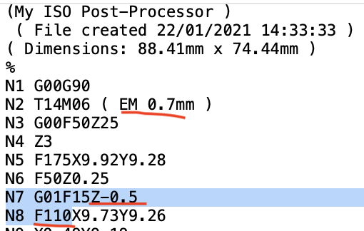
G-Code snippet:
Screen Shot 2024-06-26 at 19.21.33

Referring to my Video, this is the Milled PCB from the 1st posted Milling video and, ironically, it’s FR4. You can see the Woven Fabric telegraphing it’s pattern through the Tin Coating. Note the clean edges… some, minor rough edges that I didn’t fuss about cleaning (mostly on the PCB area for removal…)

This is a Poly PCB (Stepper Motor Controllers) - nice clean edges

1 Like

Yeah, thanks for your help – you are a great mentor.

What is poly laminate? Where do you get it? That is new to me as I have used fr4 for decades and never needed any other laminates except higher-tg variants for lead-free board reflow.

What do you use for tin? I used an immersion tin way back when I etched boards. After the nasty etching, removal of the photoresist, and all that drilling with a crappy dremel drill press, they just needed a buff with a green-scratch-pad and a few secs in the tin bath. Wow I did way too many boards like that and I will never etch again. Looks like some milling in my future though.

The “slivers” I am talking about are the places where the tool did not go completely between the pads of the 2mm connectors or the 0603 – I ensured that these footprints had 0.7mm clearance yet the path did not go between the pads and left shorting remnants. I am unsure if there are things to tweak for path generation. The small islands are different; many could be eliminated with proper routing in kicad to push the traces together just enough. However, if there was such a thing as an inverse-pocket, it would clean up everything between the traces. These traces were all selected and were milled as a profile/outside which is pretty good, but leaves some slivers to cut out and trashes the ground plane thermal spokes. If I select all the traces plus the ground plane, it routes out all of the desired copper and leaves the undesired copper, hence my inquiry about an inverse-pocket. This would also leave the plane thermals. May not be available.

I hope this does not get flagged as too non-kicad :slight_smile:

Ahh, that was silly – the ground plane thermal spokes should just get removed and then that milling issue goes away. Simply set plane zone properties in kicad for solid instead of thermal spokes, and clearance to 0.7mm (endmill diameter).

1 Like

I have some interest in PCB milling too I once got as far with Flatcam as to generate milling vectors and load those into bCNC and from that I concluded that Flatcam is much more difficult to use then it should be, and it has some nasty quirks such as leaving little triangles in many area’s where “multi circumference routing” comes together. At the moment I also have to fiddle around with a Beta version of Flatcam to get anything to work, and unfortunately there does not seem to be much of a community around Flatcam. (No, I’m not interested in CopperCAM).

I have difficulty with watching though a 17 minute video without comment, the format does not work for me. I did notice you had to select all pads individually in FreeCAD (V0.21.2 (FreeCAD has not reached V1 yet!)) @10:00 into the video. This becomes a real bore quickly on a larger PCB and is also very error prone. Is there a way around it?

Another topic which would be very nice for PCB milling is if the software could be set to “push though” area’s like in the picture below. This would make pads narrower, but that is better then leaving shorts.
image

Also, it would be nice to have an annotated index in the comment under the video, so you can skip quickly to a particular step when one of those steps is not clear.

@teletypeguy , @paulvdh

  1. PCB materials:The most common contains some FR4 in different flavors - I like the ones with Bakelite. They are Brown. Others have different materials in combination with FR4. and some, well, see image below and do some internet searching. You’ll find Polyimide among others.

I’ve used/tested plenty enough to prefer those with Bakelite (Brown). Screenshot shows FR4 and FR4-Bakelite - (Brown) you can see the layering and they Mill great. (Green-ish) Notice the visible fiberglass and no layering on these - I avoid them.
This link to Amazon is for the Brown stuff

  1. Tinning: I make my own - here’s link to my Video

Item Selection (the Track, Pads…etc) I am able to Window-Box and select that way, but doing it depends on the computer setup - I use a Mac.

Regarding my Video’s: I cater to myself and do it for fun, not really caring about what other’s like/don’t-like. 8-Billion people on this planet and I receive plenty of emails from folks that like my videos. Once in awhile someone will comment about not liking them but, I’m not interested. I did include a Time-tag in the Milling video Description-text to get user to the start of the Milling. I figure if folks don’t like it, they don’t have to watch it.

Color bleeding in graphic’s can be misleading… I turn on/off Visibility the various items as needed…

Showing how simple it is to select multiple items for milling… there are several ways to do it… curiosity is an Engineer’s best friend…

Naturally, I could have selected sections of interest and/or used Key_Strokes to select multiple items… that’s just plain computer stuff…

A better image…

That’s a Level for my Telescope (actually, anything)

Final results: in a 3D-Printed enclosure

Summary: Kicad and StepUp-Workbench in FreeCAD is a great combination - for the price ($) it’s hard to beat! (Tho, I do prefer and recommend CopperCAM for PCB G-Code…)

I asked about this on the freecad/path forum and a fellow suggested that the not-plowing-between-pads issue could be related to tolerance/rounding. Reducing the mill bit size in freecad to 0.699mm did not help, however, when I set it to 0.690mm it works as expected:

The clearance between pads in kicad is still 0.7mm, and the physical endmill will be 0.7mm, so this is just a little trick for the path algorithm.

Sometimes tricks are needed, same with Kicad, too…

Also, turn On/Off visibility of the PCB, Model…etc to hide/stop color bleeding… Bleeding happens when two surfaces are very close together and the Graphic’s bleed. Has nothing to do with the Milling except in that it doesn’t make sense to Mill very shallow depths because of CNC machine Backlash (in X,Y and Z) and accuracy, such that the bit may not get to the exact same depths of cuts.

Graphic below shows bleeding with various Visibility’s On/Off, and it would be worse if depth of cuts were too shallow. Remember, the ‘Result’ is the ‘CutMaterial’ item, the other files are not a part of the Results…

And, perhaps you’ve discovered you can turn On/Off Step-Model visibility and change colors

1 Like