Im new to KiCad, and am struggling with MOSFETS. I have a schematic which uses logic levels to switch a 2N3904 transistor that switches a P-Channel MOSFET on and off (NDP6020P). I have the data sheet and I cant seem to find either a generic or specific symbol for the MOSFET. Here is the symbol from the data sheet:
OK. I’m looking. They only have pin numbers but I think in every possible configuration. That is the important part. You need to match pin numbers to the correct function.
From there you can mirror it top to bottom and suddenly one of the library symbols will look like this one.
Well, there isn’t a topic for both. Since choosing the right symbol is heavily dependent on the part package, the category does fit.
I see in your original post that you have a specific pMOSFET part number. You will need to get a hold of the datasheet for that part because you need to know which pin number is which pin function. Several models of mosfets that use the same package may not agree on pin number to function, and the same model in different packages may have different pin-outs as well. If that model has several packages, you need to decide on which one you will use. The symbols in the standard libraries are labeled SGD, DSG, etc. Those are the pin 1, 2, and 3 order. So for the first example SGD, pin 1 = Source, pin 2 = Gate, and pin 3 = Drain.
A trick that you can use is if you are using multiple mosfets of the same type in your design, place one mosfet symbol. Then immediately get all the settings correct (footprint, ordering information, etc). Then copy that symbol as many times as you need it. This helps reduce the amount of duplicated information that you have to type in. (You can apply this technique for all other components.)
There are many more N-channel FET’s then P-channel fets, but that is to be expected.
Do you have the libraries installed?
@Rene_Poschl With the description of some of the P-Channel Fet’s Id and Vds are negative values, but with others they are positive, which is at least an inconsitency in the libraries.
The NDP6020P is available in THT TO-220 and SMT TO-263AB (the missing centre lead variant)
The first decision is which package are you using.
The select a suitable footprint and work backwards to assign DGS or GDS etc
Some manufacturers quote negative voltage and current values for PMOS and PNP devices, it makes filtering a range a real headache on distributor websites
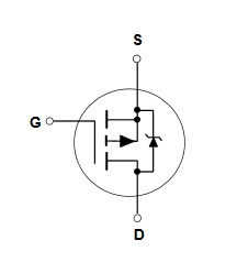
It’s PMOS_GDS. Bear in mind symbols shown in datasheets aren’t necessarily in the form you expect. In this case they have shown the symbol “upside down” with respect to its normal usage in a circuit.
That is an inconsistency in the industry. I believe it arises from two different conventions for defining the sense of a current:
Consider the device in its “normal”, intended, biasing conditions. Define current sense according to the most common practice in circuit theory - i.e., current flows from the more positive voltage potential to the more negative potential. With this approach, both N-channel and P-channel devices (as well as NPN and PNP) have positive drain currents under normal operation.
Define the currents with respect to the device (or its package) without regard to external circuitry, biasing polarity, etc. The most common convention is that current INTO the pin is positive, while current OUT of the pin is negative. With this approach, N-channel (and NPN) devices have positive drain currents, while P-channel (and PNP) devices have negative drain currents.
There are examples of both approaches on distributor web sites as well as manufacturer data sheets. When you first encounter the two approaches side-by-side, it seems confusing or even incorrect. After thinking it through, you learn to accept it (at least on an intellectual level) as simply a quirk in the “personality” of this profession.
paulvdh thanks for responding. Yes I have the libs installed. I have selected every pmos on the list and non corresponds to the data sheet diagram unless I’m missing something else.
SenbazuruCDE, I have the ON Semicinductor data sheet and the pins are not numbered. They are only labeled by function (G,S,D). Is there a generic pmos that could work? I’m not an engineer, just a hobbiest. This is so complicated.
This does NOT mean that all of these configurations are currently manufactured; it is only a reminder to me that a manufacture could throw a wrench into the works if they wanted to.
The first letter is possible Pin 1, second letter possible Pin 2, and the third letter is possible Pin 3. A devices physical pins are typically given a standard numbering scheme for each package; I won’t otherwise mention that some manufactures consider tabs the same as pins.
No, they are just upside down.
Print out the datasheet on a piece of paper and hold it in front of a mirror to view it. The functionality remains the same, despite how it visually appears.
It only changes how the symbol is oriented in the schematic. (Same result as if you drew a new symbol that is mirrored but with the same pin assignment. KiCad includes a mirror function for symbols as this is a common use case that does not really require new symbols to be drawn -> makes the same symbol able to be used more flexible and therefore gives the circuit designer more option on how to draw the schematic.)