Nightly Kicad gerber files don't pass PCB manufacturer tests

I’ve got a strange error from my PCB manufacturer after I upload gerber files I generated with Nightly Kicad build - “Solder Mask Bridge error Measured 200μm, Optimal >250μm”

1

The last time I generated and upload this project’s gerbers files was in March 2020 and there is no any errors.

There is the difference between old and new gerbers.
See posts below because limit 1 picture per post for new users.
As a new user I also can’t attach gerber files.

How to fix it? Any ideas?
Is it a bug?

How to make mask layer solid?
May be there is another workaround how to pass my PCB manufacturer test?

old-F_Mask.gts - when click on the QFN-24-1EP_3x3mm_P0.4mm_EP1.75x1.6mm mask selected area is SOLID

G04 Gerber Fmt 4.6, Leading zero omitted, Abs format (unit mm)*
G04 Created by KiCad (PCBNEW (5.99.0-1018-g3c1970434)) date **2020-03-06** 12:17:32*

!

new-F_Mask.gts - footprint mask is not solid, it contains multiple shapes

G04 Gerber Fmt 4.6, Leading zero omitted, Abs format (unit mm)*
G04 Created by KiCad (PCBNEW (5.99.0-8027-ga572be54e1)) date **2021-01-11** 23:16:10*

!

In case you ask there is my export setting but I tried other variants and result is the same

!

What are the mask clearance and min width values in board settings, footprint and pads?

I’m a bit out of my league here. I try to avoid such small pitch components and do not design enough PCB’s to have real experience in this area, but I try to write something that makes sense…

Your QFN (I think) has a pitch of 0.4mm, which only leaves 0.2mm for the pads and their clearance each, and at that resolution it starts to become difficult to put the soldermask reliably between the pads.

By default KiCad has a “Solder mask clearance” of 0 (I think) and this means the solder mask has the same pad size as the pads, and this is something I do not understand well. The result is that the exposed copper area of the pad gets smaller with any misalignment between the copper layer and the solder mask, and this is not logical to me. I do know though that a lot of attention is put into KiCad’s libraries to follow IPC guidelines, but it’s a conflict in my head for which I do not have a solution.

You can set a global variable for this in Pcbnew / File / Board Setup / Defaults / Solder Mask/Paste / Solder mask clearance: You can also override this global value for individual footprints or individual pads.

And then it starts becoming more difficult:
There are ideas like SMD (Solder Mask Defined pads) and NSMD Non- SolderMask Defined Pads:
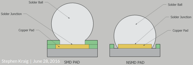
image
Source (with explanation):

By using different sizes for the mask and the copper, the size of the exposed pad stays the same if there is misalignment between the copper and the mask, and this results in a better defined soldering process. Macrofab uses BGA’s, but the same is true for and SMT footprints that are soldered with reflow, and therefore have a fixed amount of solder on each pad.

If you want to use Solder Mask Defined pads, then this probably means that you want to make the copper of the pads wider. In your case around 0.25mm, and if it’s difficult for your fab to make the 0.2mm “fingers” for the solder mask cutout, the mask can be made a bit smaller (for example 0.18mm), which results in thicker “fingers” of 0.22mm. (My numbers are just an example, NOT based on experience nor guidelines).

Changing the mask clearance is quite easy in KiCad, but for changing the size of the pads themselves you have to modify all the pads of the footprint.

Here is my board settings

This is for the footprint. Didn’t change settings for pads.

Do you need more?

Also I would like to notice that settings in both cases ( new-F_Mask.gts and old-F_Mask.gts) is the same. The difference only Kicad versions. It is the same project.

old-F_Mask.gts - passes all PCB manufacturer tests
new-F_Mask.gts - don’t pass

Thanks.

My manufacturer recommend “expansion, Solder Mask Swell - 0.050mm”
As I understand on your picture it is “NSMD PAD”. Not sure they accept “SMD PAD” type.

Not sure I understand how to use this information in my case. old-F_Mask.gts - passes all PCB manufacturer tests. The same settings just different Kicad versions. Before changing pads and mask size I would like to understand why old-F_Mask.gts - passes all tests. I didn’t change anything.

O opened old-F_Mask.gts in Gerbv
I can select footprint’s shape and delete it. Shape is solid.

new-F_Mask.gts in Gerbv
Shape is not solid. I can select objects inside footprint

I think this is the main reason why new-F_Mask.gts don’t pass tests.
Could you explain me how to make footprints’ shapes solid again like in old gerbers?
Should I change some options for it?

old-F_Mask.gts - https://pastebin.pl/view/e1ae2515
new-F_Mask.gts - https://pastebin.pl/view/19727632

What if you do NOT merge the mask openings, but tell your fabricator that he is allowed to merge them when the pad to pad clearance is less than x? After all, neither you nor the assembler wants the openings to be merged. You only do this to make life easier for the fabricator.

You could also not spread the openings, but have openings = pads. You do not want bigger openings, that is only so for the benefit of the fabricator.

Genrating the Mask layer gerber looks buggy. Here’s what I get with the same settings.

image

The fact that it’s not one solid object shouldn’t be a problem in itself. But the handling of pads has been changed recently and apparently mask handling was changed, too.

EDIT: I’ll report this.

I have to take this back. What you see is what you should expect with that footprint. The horizontal and the vertical space between the thermal pad and other pads are different in that footprint (I thought that was a bug). But there are some small problems, see the screenshot in https://gitlab.com/kicad/code/kicad/-/issues/7093.

I don’t know why we have different result, you have solid areas while I have separate circles. Maybe the footprint has been changed. Upload exactly the same footprint which you are using if you want us to check it.

You have different solder mask layer because you use current QFN-24-1EP_3x3mm_P0.4mm_EP1.75x1.6mm footprint.

I created this project in 2019, since 2019 there was several changes in this footprint. Also I added thermal vias.

I did experiment. I created a new project with current QFN-24-1EP_3x3mm_P0.4mm_EP1.75x1.6mm
version footprint with my settings and it also didn’t pass the manufacturer test.

After it I changed:

  • Footprint Settings: Solder Mask Clearance in footprint settings - from 0.06 to 0
  • Board Settings: Solder Mask Clearance - from 0.051 to 0
  • Board Settings: Solder Mask Clearance - from 0.25 to 0.2

It passes tests. Now it looks different of course.

Well… Probably when I set these setting in 2019 I didn’t fully understand what it do exactly.

I still didn’t understand why old KiCad gerbers passed the test but same project with new KiCad didn’t pass. Because I fix this problem it is OK for me for now.

Openings = Pads is a best practice? Right?

I don’t remember why I set it 0.51, probably got some warnings and read on manufacturer web site “expansion, Solder Mask Swell - 0.050” and set “Solder Mask Clearance - 0.051” … But somehow it is pass test with “Solder Mask Clearance - 0”

As I understand “expansion, Solder Mask Swell” and “Solder Mask Clearance” is the same thing.

Here’s a bit more about the mask layer: How does solder mask layer work?.

Can you give a link to your manufacturer’s recommendations or instructions?

Thanks

This is my manufacturer’s recommendations:

https://www.rezonit.ru/directory/tekhnologicheskie-osobennosti-proizvodstva/

It’s a typical table of values. Notice that it describes their capabilities (i.e. what they can do), not what you should do. It’s impossible to say from that table alone if they want you to use those values for generating gerbers or if they will use those values to modify your gerbers if you leave them to zero. That’s regrettably true for many other manufacturers, too. If you can afford, you can order a prototype with zero values and see if they adjust them to their recommended values. Or just ask them, if the information isn’t found in their website.

1 Like