Ive looked at other posts on this but don’t have enough understanding of what I have done wrong cant get rid of this error.! am trying to recreate this mfos power supply schematic.
http://musicfromouterspace.com/analogsynth_new/WALLWARTSUPPLY/WALLWARTSUPPLY.php

i have added a pwrflag but am still getting two type 3 errors what do i need to add to the inputs of the regulators to signify the input

I missed it before because of the scale. It might have been helpful had you circled the green arrows in the first example to highlight them. Probably the diodes between the Power Flag and the input are causing a problem would be my guess.
Unfortunately KiCad isn’t intelligent enough to understand how the circuit actually works. The net in which the regulator input is must have its own power symbol. Wouldn’t it be nice if KiCad would actually know that if there’s +5 power source the diode lets the current go trough. But it would mean that there should be information about all components, not just diodes. It would come close to spice modeling.
This can be subject to opinion. I would add the needed PwrFlags to the right side of D1 and D4.
Thank you for your help, understanding the circuit on paper and then bringing into software turns out to have a bigger learning curve than i expected
Quite simple, and simpler than you would think.
- Remove the PWR_FLAG from J1 pin 1 net because this is already flagged by that AC source provided that AC symbol is defined accordingly.
Add two PWR_FLAGs.
- One to U1 pin 1
- One to U2 pin 2
They can be placed anywhere along each of those nets.
You basically flag each net as a ‘power’ receiving net.
That’s all.
I would assume the AC symbol is a simulation only symbol. It must be setup such that ERC does not take it into account for being a power source as it really is not one. I am not even sure that simulation only symbols can be mixed into normal pcb design schematics as i am uncertain if one can use the # refdes prefix trick to ensure it is ignored by the “netlist” generator while still being able to simulate (i did not yet play with simulation).
If it has the pin type power out then it would be a mistake for exactly this reason. (power can only come from real components not from simulation parts)
I got confused! The AC symbol is not a simulation symbol. It is a power symbol. Power symbols are defined with a power input pin not a power output as the pwr flag provides. So no you can not remove the power flag near the connector.
@jdark are you aware about the fact that the AC symbol shorts out your two connectors (J1 and J2)? (Assuming it is the AC symbol taken from the official power lib. Use highlight net to check this)
Also look at J4 and J3. They seems to be unconnected (could be an artifact of the screenshot).
I checked against the power library where it is declared as a power symbol hence shouldn’t need an additional power flag.
Am I missing something here?
You should read the FAQ article linked above as you clearly do not understand what the distinction between power label and power flag is.
Aha, that’s what it is. Label vs. Flag.
In this case that AC power label stays of course. 
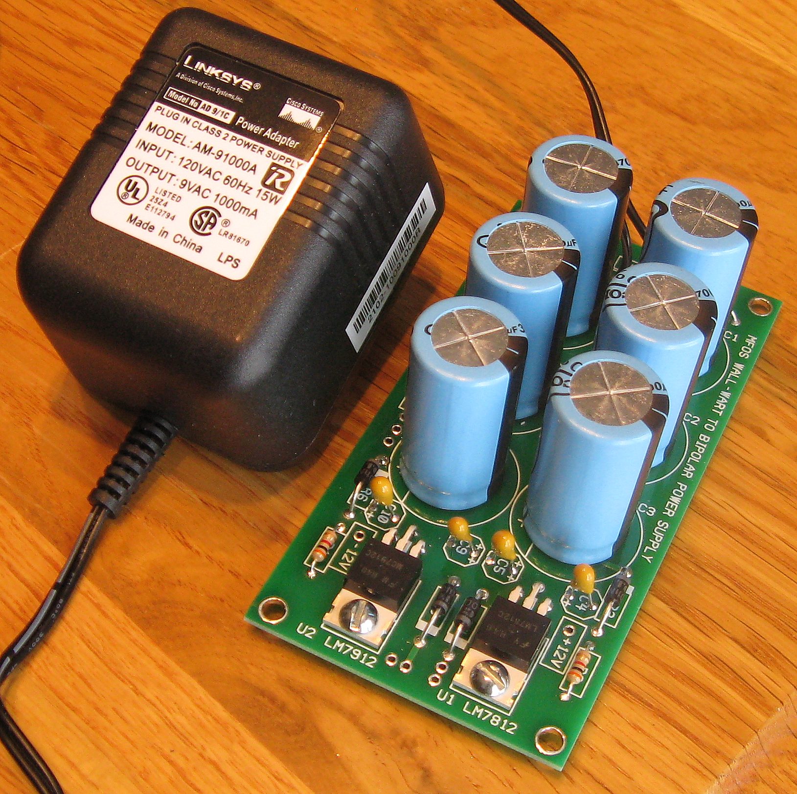
Ahh okay so in the original schematic that I am trying to replicate the input is 12v ac going into j1 and j2. J3 and j4 are my outputs but think i have labeled them incorrectly. Here is a screeshot of the original.

As already mentioned.
PWR_FLAG each on CR1 pin k and CR2 pin a, or whatever diode you may use.
Never mind that AC Label thing earlier. It’s a different issue.
Well if done correctly then there will need to be a power flag on J2 as well. (right now connecting this system to the external power would short out the supply!)
I would also suggest some sort of over voltage protection on the input. (Right now any over voltage will damage parts probably starting with the caps.)
It gets even better. If I was a diode on 18.8 mF without any inrush control I would sign off regularly. Then those together as 37.6 mF on some supply without even a ptc. Good luck with such design.
In fact going by that picture it seem that this 1A power adapter acts as a ‘safety feature’ due to its limited output capability.
Sorry for my late reply, my internet was out of service during the last few days.
Isn’t the PWR_FLAG, connected to GND, not shown on the schematics above?
But I guess, Jdark knew about it and added it.
This topic was automatically closed 90 days after the last reply. New replies are no longer allowed.