IMHO this is not “simply asking someone else to design a footprint for me”.
Using the 3D-Viewer for the first time, I noticed that my choice of “2x19 pin headers” is fine for the PCB (everything works fine), but in the viewer I see, well, pin headers although what I’m going to solder there are pin sockets.
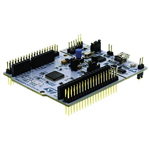
Changing the footprint to “pin socket” does not work, because if I do, pin 1 is on the wrong side. I don’t know if this is unusual, but I want to plug this into two 2x19 sockets. As you can (barely) see, it has pins on its back. This means that pin 1 of the “double sided” pin header on the Nucleo-board should go into pin 1 of the socket on my PCB. However, the only footprint available for pin sockets in the library has pin 1 “on the wrong side”.
I suppose you could argue that this is a “cross connection” and therefore I should exchange even/odd pin numbers in my schematic. But if I do this I’ll end up with a very confusing schematic.
Since these pin header footprints show up as “generated”, wouldn’t it be useful to extend the generation to also have pin sockets with pin 1 “on the other side”?
If you want pin 1 of a header to mate with pin 1 of a socket, then the numbering in the library is correct.
The board in your photo, with header pins extending through the board, the pins on one side will be numbered properly while the pins on the other side will be numbered backward. This is an unusual situation and having library components with non-standard numbering would be very confusing.
When stacking boards it’s much more common to use a connector with extended pins so that there are pins on one side and a socket on the other. The PC-104 design uses this style connector.
Mating connector pin numbering has always been a minefield. I got bitten a couple of times with DIN 41612.
30+ years ago at Racal we had an internal standard of main card, back plane with pins on both sides and an interface card on the back. The backplane had sockets on both sides with mirrored pin numbering. In the end pin 1 connected to pin 1 all the way through.
Is this a case where one connector is on the Top of board A.
The mating conn should go on the Bottom of pcb B?
If you are using plane headers and sockets, there are no pin numbers on the physical conn (like Canon D). You should be able to Flip the connector to the other layer and the pin numbers will reverse.
I accidentally bumped into this thread from over a month ago.
A quick and dirty fix would be to simply link another 3D model to your footprints.
But this ignores the underlying problem with the pin numbering. If you exchange a male for a female socket in the same footprint, then the pin numbering is simply wrong and this easily leads to errors later in the design.
If I try to back to the roots, then
So why would this create confusion in your schematic?
Try this:
Open Eeschema with your project.
Hover over the connector (no clicking needed)
Press m for move. (This attaches the symbol to your mouse cursor and detaches it from the wires)
Press: r (rotate) x (mirror in X-axis) and y (mirror in Y-axis) until it looks good.