I designed a couple of circuit boards and I want to get them manufactured but so far 3 out of 3 places that I’ve contacted told me that the track spacing/clearances are not up to spec.
The spec calls for 8/8 for the smaller board with 0.5mm drill holes, I might be mistaken but I figured 0.8 mil was essentially the same as 0.2mm which is the spacing I used since I’m more used to working with metric.
I’ve tried two online DFM tools but so far they haven’t really shown anything that I’ve been able to perceive as important, I guess I could go back and change all spacing to 0.2032mm but given the amount of work I’d rather not, any ideas or suggestions?
Github Project Link.
I’m sorry if this is a stupid question but I’m relatively new to PCB design and still getting the hang of this.
I like the looks of tighly packed parallell tracks, but this example above screams DRC issues
What routing mode do you use for the layout?
EDIT: indeed changing to 8mil spacing will get you plenty of work.
Unfortunately 0.032mm matters for the fabs. Have you tried with PCBWay? I use their services for short runs/prototypes, and they did not have problems with smaller clearances. 5/5 no problem for them.
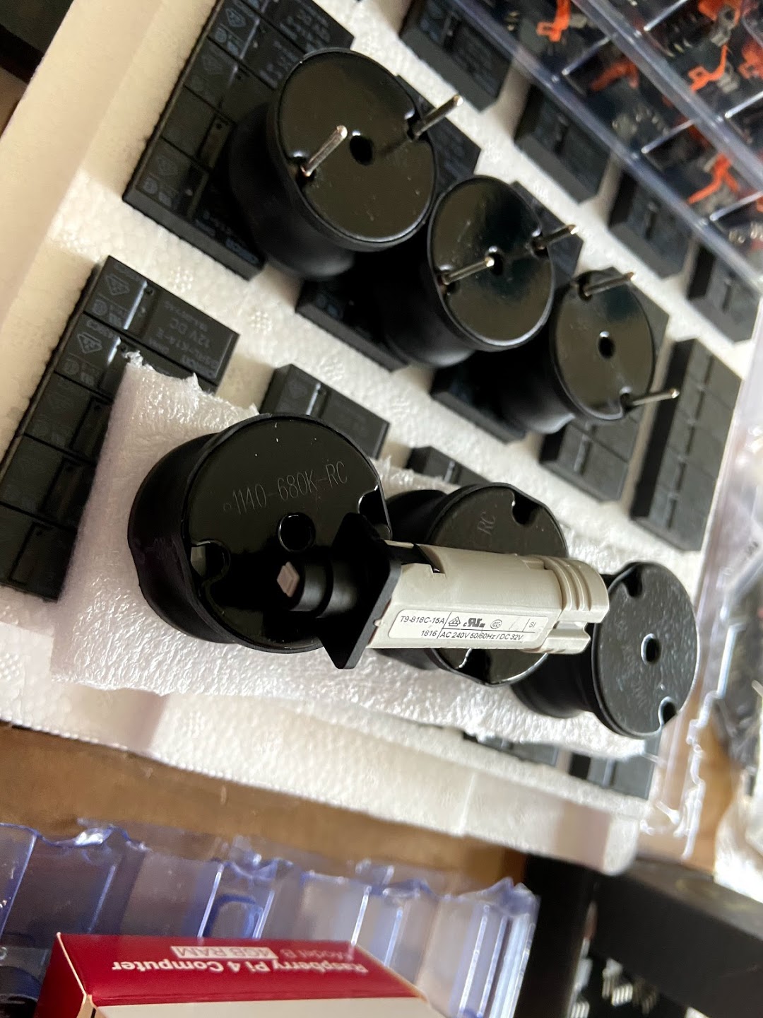
Thanks for responding, PCBWay is actually my preferred FAB at this point, the issue is that due to rather high currents (up to 60A) I Have to go with thick copper layers which again restrict minimum trace width and spacing (6oz for the parent/main board and 13oz for the smalller daughter board).
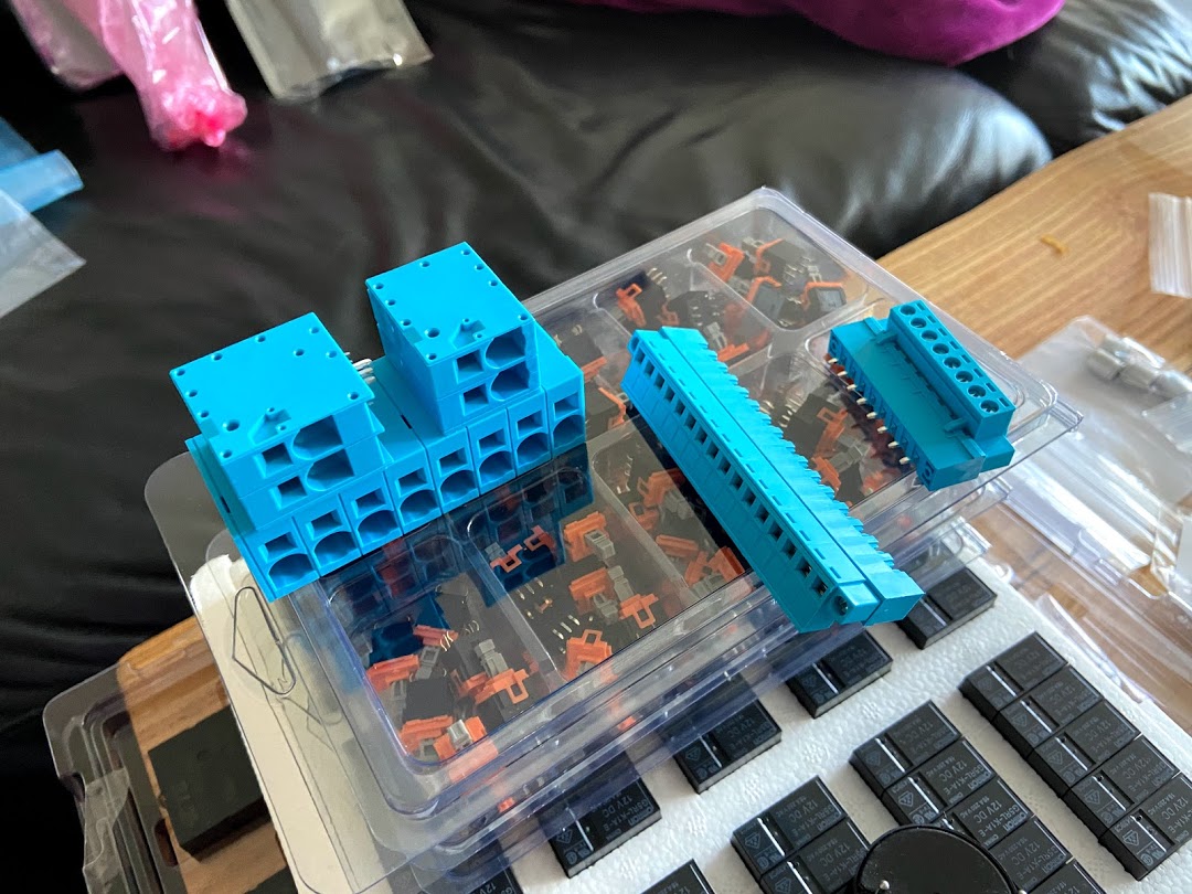
I’d probably also have to remove any connector with .2mm pitch and swap for .254mm so I can route in between the pins for the signals.
Thanks for spotting the missing trace there, seems while working last night I deleted the trace that connects the left and the right side, thx for spotting that.
@antevens I don’t have much experience with high current designs (my designs usually don’t exceed few amps), but as I read 6oz is problematic (=expensive). I’ve seen some practical suggestions to switch to 4-layer 3oz boards to make the boards easier and cheaper to manufacture. Have you considered that?
According to my calculations (I don’t know much about this other than what I read online)
60A over 300mm (biggest/longest traces on the larger board) would require 14.2mm total trace width for outer layers assuming 6oz so 8mm on each side should be fine and I’d only loose about 0.1v or 6W under full load and board temperature would go up about 10 degrees C.
If I switch to 4 layers then the internal layers can’t get rid of heat nearly as well as the outer layers so I’d need closer to 74 mm in total if everything was done with inner layers.
Assuming I use traces on both outer layers and internal layers that would mean that total trace width would have to be around 10mm ( 10+10 outer and 10+10 inner). It also becomes a bit problematic to design around connectors and pads ensuring enough clearance while routing thick traces and making sure they can be soldered.
It might be doable though, going to try to estimate the cost of going that way
Thanks for the feedback, going to go back, swap out out the 2x20 metric connectors for the imperial 2.54x20 ones and re-trace the whole thing to pass 8/8.
8mill clearance dos not combine with 6oz copper.
1oz copper is around 35um thick, so 6oz will be 210um, which makes the troughs between the tracks deeper than their width.
Those 6/6 or 8/8 standard rules only apply to standard copper thickness.


