Hi,
Sorry if this topic exist, but I can not found it in the forum.
I want to put a LCD in my board. The LCD is a standard 16x2 character display, paralel protocol.
When I put only the LCD, in schematic is fine, but in 3D appears “floating”. So I need the pin headers, male and female. That’s good because I need them in the BOM too.
This is the only way I know to make electrical connections “upper” to board.
If I put in schematic a simbol for pin headers, in layout I have these footprints, but these footprints are the same holes for the LCD footprint (i mean same holes for electrical connections). I think is not correct put a footprint over on another footprint.
Whats the correct way to make this?
The final solution should have a schematic with clearly connection to LCD, layout with only LCD holes but in 3D view with headers in a proper location.
TIPS: LCD layout has a mounting holes, that I need too in layout. The final BOM should have all the components needed for mounting so i need the pin headers appears in it, and 3D view is only for create a documentation of the board.
I use a variety of Displays and generally don’t fuss with ‘ideal graphic’ representations in PCB or Schematic. I prefer to somewhat generalize them thus, enabling not being tied down to exact features until ready to do so.
The attached is the 16x2 LCD I use (.step, .wrl and .mod). You’re welcome to use them but, rather than including the Symbol for the Schematic, I leave it to you to make - very simple to do and assume you’ll do homework on how/where to place files and use them.
Making the 3D model (.step, .wrl) and attaching PinHeader would, perhaps, be more challenging to a newbie as it’s done in combination of Kicad and FreeCad/other. So, I include them for your peace of mind… But, I encourage learning how to do it…
Note: The Graphic for the schematic is done in Eeschema editor and can look like whatever you want to draw. Just add the Pins and associate the Footprint with the graphic. Screenshot below…
The way I interpret the post is that DavidH wants both the LCD and the connectors for it in the BOM list, and as far as I know KiCad does not really support that. It’s one item on the BOM for each schematic symbol. You could interpret the BOM entry for the LCD as an “assembly”, but that would be around KiCad itself.
You have to draw a border somewhere. your PCB probably needs screws, washers, a housing to put it in, cables, connectors, a box to ship it to a customer, etc.
No details about LCD were provided - pinheader location, I/O typed… (they come in different flavors/locations). Some have only 14 pins, some 16 pins… Some with I2C.
BOM needs are inferred, I assume because user does not know how to make footprint with PinHeader attached. Again, no details…
I have 5 drawers full of a variety/brands of these guys and, for me, deciding which to use on a particular project is the challenge.
Image below shows New unit in package. It has Header & I2C attached. Cost was 2 units for $6 on amazon…
Regarding the BOM: Obviously, an LCD with attached pins would be a single-unit. But, if user wants it separate, user will need to make model that way (or, specify exacactly what’s wanted so a forum reader can avoid Mind-Reading…
EDIT - forgot, There are two ways to get a BOM (as you know): 1-via Schematic, 2-via the PCB Fabrication Output (menubar…) So, even without using Schematic, a BOM can be created that has/doesn’t-have headers,… as user desires…
Also, though user did indiocate ‘Parallel’ I/O, we know that many folks (especially newbies) use words that may not correctly indicate what’s wanted and replay words in sales/ad’s…
I can only talk for my personal solution. First 3d:
You can add more than one 3d model for each component. E.g. you can have a 14-pin IC. But you can add also the model for a 14-pin socket and raise the IC a few mm to get a socketed IC.
BOM: for me, the final BOM is in my ERP database. So I have an article like “Display with connectors” wich contains the Display, its pin header and the socket (and additional mounting parts) and I use this as a sub-BOM. So, the Kicad BOM contains only one article but the buyer knows there are three (or more).
Hi again,
first sorry for my less explanation. I was preferred doing generally to help another people in the same question.
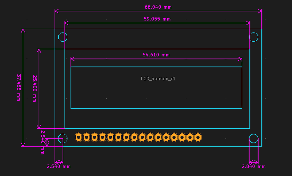
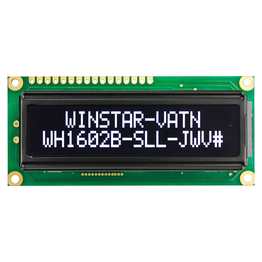
Consider that the LCD is this: LCD Winstar
The LCD will be purchased directly from distributor and comes like the image. I don’t know any version with headers soldered that can be purchased from distributor. I’m talking about 100 units/month, so amazon’s versions is not a choice.
Paulvdh understand me. The solution proposed by Robert_Loos is not good for me, because our ERP doesn’t manage the contents of the PCB. In the past, with another program was not kicad, I sent a BOM and a list of instructions with materials to make the final board.
My objective is make a BOM with all items needed and a simply 3D view to understand how to build it.
The BOM will be created in Kicad is build with pcbnew, with a plugin that generates a interactive HTML BOM.
I think that the only way is put symbols in schematic for male and female headers, without connections.
In layout, leave these footprints out of the board, and in 3D view, export to step and with other 3D software move the header in the proper location. But i’m not sure if gerbers will be ok if there is components out of the board.
Comments:
• BOM’s from Eeschema require a File Path which must be done by user (or by using some plugin I know nothing about). Also, output shows paths and, most likely you wouldn’t want them…
• Making Graphics for Eeschema is simple (5 minute screenshots below) and can include imported graphic
• User Chooses what items to place thus, what gets included on BOM
• 3D Footprints can be associated with the Eeschema symbols as user chooses
• 3D Footprints are available on internet from many sources or, can make your own from PCBnew Step file; exporting desired items, such as PinHeaders, Screws, Washers…etc
I prefer to not abandon you but, my old, slow brain informs me getting what you want will require several posting / iterations, which I’m not keen on doing but, others may… I think enough info is posted to help you along this path…
Hi again,
I found a solution that helps me.
I made a new symbol in schematic called “empty” and drawed a little square without pins.
I made a new footprint in pcbnew called “empty” and drawed a little cross in fabrication layer, no more in other layers.
Now, in my scheme, I can put a empty symbol, with my custom value “Header 1x16 2.54”.
In pcbnew, now I have footprint with no pads. The gerbers doesn’t affect by this new footprint. Now, with the coordinates of pin 1 of LCD, move the empty footprint at this location.
And now, this empty footprint set the 3D view to a Header 1x16 2.54.
After all, I have a new component, appears in BOM and in 3D view but no changes in PCB.
The only problem is put male and female in the same coordinates X and Y, but different Z. But this is my best aproximation.
This is similar to a solution that I came up for myself for socketed ICs on one of my collaborative projects. I created a bunch of symbols for sockets, one for each pin count that I was using. I then put the correctly sized socket next to the power unit (and bypass capacitor) on my schematic.
Not only does this include the sockets in my BOM, but also adds information to my schematic for the pin-count of the IC and which ICs have sockets.
For the footprints I did something that at first brush seems a little counter intuitive, but made sense to me at the time. I assigned the socket footprint to the IC symbol, and a new custom IC footprint to the socket. The custom IC footprint is a copy of my standard library IC footprint with the pins and courtyard deleted, and the 3D model of the IC raised in Z to match the height of an IC in a socket instead of an IC in the board. My reasoning is because the socket is what actually connects to the board (and may have slightly different pin geometry, diameter, spacing, etc than an IC package). Here is a pair of screenshots showing the same ICs in the schematic with all 4 IC parts next to each other: (If you click to the full-size view of the PCBNew screenshot you should see the blue crosshair for the insertion point of the XU? footprints. In this case because it is for THT IC, the insertion point is where pin1 will be on the finished board.)
You could certainly use a similar technique for the header strip for your LCD module.
Note: For this example I put the Ref’Ds (reference designators) where they can be seen in my example 3D views. On my actual board I have the XU? Ref’Ds in the middle of the footprint so it is only visible before putting the sockets in the board. I also have the U? Ref’Ds closer to pin 1 as additional on-board documentation for the location of pin 1 because once the board is loaded with components it is harder to see the square pin 1 and also harder to see the notch in the silkscreen.
•The class letter to use for common hardware (screws, flat washers, lock washers, nuts) is “H”.
•The class letter to use for a display of any kind is “DS”.
•The class letter to use for a header of a display (either pins or sockets) is XDS#.
•If you happen to use two single in line headers (sockets or pins) to mount a single device, say an assembly A1. Then the headers would use ref des of XA1A and XA1B. However, KiCad does not understand individual items with suffix letters so use XA1E1 and XA1E2 (to fool the system).
–Larry


