When I try to trace a ring around sensitive nodes for guarding, they get deleted as soon as I close them.
Even when I put pads or vias in the ring to break it into segments, it will still be deleted?
How to prevent this ? And also: Why was this “feature” ever considered useful ? If I lay out multiple routes between two points, then there is always a reason for it.
I do find it a useful feature to turn this on.
It quite often happens that I have routed a track between some pads, and then discover I have to move it. For example to route it around something else, so that “something else” can be reached from the left side instead of from the right side. In such a case I just route a track around the right side, and the track on the left side gets deleted by KiCad.
But different people have different wishes and work methods, and therefore you can configure KiCad and tell it to behave in the way you want it to behave.
I found the option exactly where you described it to be! This option however is not listed under the regular Preferences menu (where I was initially looking for it)
I recommend that every now and then you take some time to read a part of the documentation, or start a bogus project (copy of a real one?) with the sole intention of exploring the menu’s in KiCad and experimenting with what happens if you click on menu items that are unfamiliar.
Make some notes if you find useful functions.
It’s also why some people like GIT so much for KiCad (or another good backup strategy).
It gives them ease of mind while trying out new things they are not entirely familiar with.
If it goes wrong, and Undo does not work you can alsways revert to the latest backup.
For several reasons I’m still under version 5. Shame on me !
I never had to trace a guard ring around pads but my first idea would be to use copper zones and filling option. I don’t have time to check it at the moment. Is that a bad or good idea ?
TIA
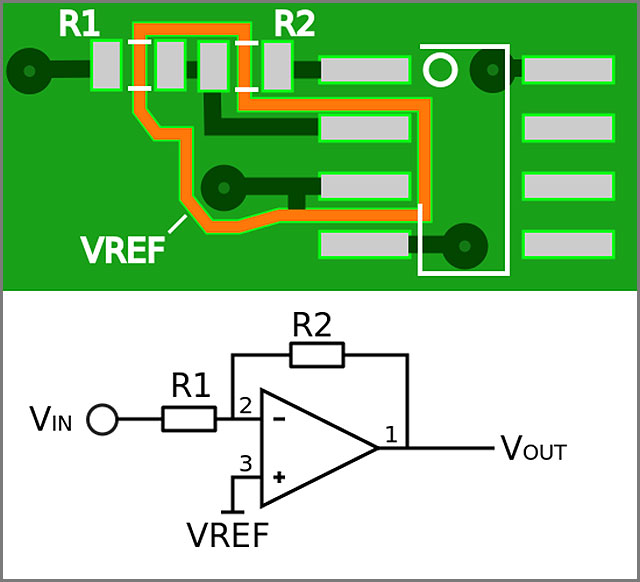
If this is a high impedance circuit. (for example R1 and R2 are both 100Meg), then any leakage current over the PCB to or from the non inverting input of the opamp will create a disturbance on the output. This leakage may occur due to flux residue or other contaminants, or just buid up of dust over time.
In the picture, the guard ring is connected to a relatavie low impedance source, and has the same voltage as the non-inverting input of the opamp. Because there is no voltage difference (or a very small voltage difference such as the offset voltage of the opamp) there is also no current flow, even when the PCB is dirty. Such guard rings always have to be exposed copper. If they are hidden below a layer of solder mask, and there is dirt on the solder mask, then the leakage can still happen though dirt over the surface of the solder mask.
In this form of a guard ring it does not make sense to use a zone. You just want a narrow but exposed copper track.
The last project I did with guard ring mask removal, I just used line segments on the mask layer (remember this is a ‘negative’ layer - ie. any feature here is removed from the mask).
But that is not a very good implementation of a guard ring.
You really want to cover the sensitive track itself with solder mask to increase isolation from it’s surroundings. Even adding silkscreen over the soldermask may improve it even further, even though silkscreen is not designed for this and there are no guarantees.
On a 4 layer PCB you can also move the sensitive tracks to an inner layer.
Using guard ring around a track on an inner layer probably is not very useful, but adding it only around the exposed pads on the surface may still be beneficial.
 I couldn’t find it Preferences → PCB Editor though.

