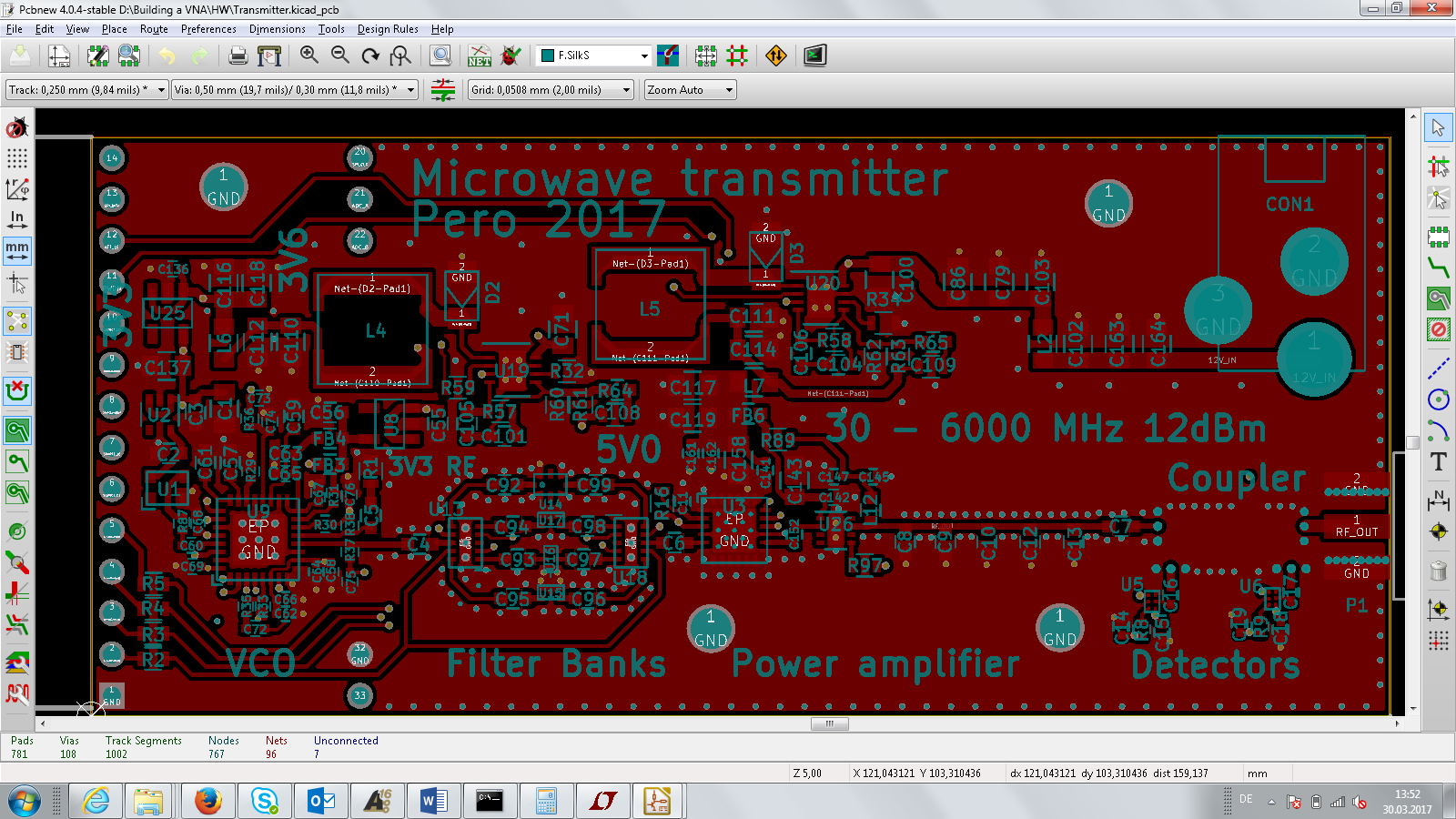
Please tell me how to place GND Via (IVH) along the microstrip line like a linked image.
https://cdn.hackaday.io/files/20350870654400/top_layer.png
(https://hackaday.io/project/20350-microwave-transmitter)
Please tell me how to place GND Via (IVH) along the microstrip line like a linked image.
https://cdn.hackaday.io/files/20350870654400/top_layer.png
(https://hackaday.io/project/20350-microwave-transmitter)
What I have found to be the easiest is to:
Create a footprint for the via or use an existing footprint from the Wire_Pads library (such as SolderWirePad_single_0-8mmDrill).
Pace one instance of it on the board using add component
Hover the mouse over it and press E on the keyboard
Select the PAD when asked to clarify
Then edit the NET field to the appropriate name (ex. GND)
Now you should have a via that you can copy and paste wherever needed that will be connected to the appropriate net.
IVH seems to be different, it can’t be done with footprints, see e.g. http://www.oki-printed.co.jp/en/product/in.html
Sorry, you are correct. There is no good way to put a multi layer via design into a footprint. Impedance control on the micro strip would need to be specified before manufacturing. This is the best way that I have found to create stitching vias without a whole lot of mess.
You don’t need IVH vias here, ordinary “stitching” vias are what you are looking for, TH (through hole) vias will probably suffice for a four layer board but for high density (and higher cost) you could use BVH (blind via holes). IVH is another manufacturing method used for high density boards to create micro vias with larger aspect ratios, therefore connecting to more layers (and more cost).
This topic was automatically closed 30 days after the last reply. New replies are no longer allowed.