How have PCB manufacturers eliminated NRE?

Sorry, this is really not about Kicad in any way, but it’s a question I have been unable to find an answer to, maybe someone here, in the business, knows…

I’ve been designing PCBs (oh, sorry, PWBs) for 50 years. Up until maybe a decade or so ago, it was always a very expensive proposition to get a board made due to the “NRE” (Non-Recurring Engineering) cost, which was mostly the cost of the photo plotted films, but also some hands-on production time doing the board stack-up and placement, etc.

These days, I can order 5 small prototypes for $2 each, with no NRE.
How are the production houses doing this? Are they not making films anymore (direct imaging)? Or, or they just combining many different jobs and absorbing the NRE for the combined layout. Or, have films become so cheap that they are basically free?

I would imagine that cheap computing power has made production much quicker, and that probably helps, but going from $200 to $0 is still pretty amazing.

Anyone have some insight?

They are still using films a lot of places. I think the cost is driven down by the raw materials being extremely cheap, and minimizing labor by batching jobs together.

I never believed that the plotted film itself was a significant part of the NRE, but it’s something that is easy to explain. It’s all the small things that add up, From the person taking in your order and data transfer (I once had a design on floppy disk that I brought to a local PCB manufacturer), some checking of the gerber files and up to packaging and shipping at the end, and all those little things add up, especially for small orders.

And a part of the NRE is simply delegated to the customer. Instead of talking to someone on the phone or reading your mail, you use the internet to upload your files, set all the production properties and use their online gerber viewer to check for incompatibilities. That already eliminates a lot of human labor on their side.

And of course economy of scale is a part of it. From bath processing and automatic nesting of PCB’s from lots of customers on a single big panel, to multiple identical panels. For example Oshpak only does orders in multiples of three. That almost certainly means they have a big drilling machine that does three big panels at a time.

I don’t now how many PCB companies still make films, but it’s also common to have some kind of photo plotter that directly plots on the light sensitive material on the PCB. It probably also depends on their specialization. For big batches, making a film seems more appropriate, while for one-offs direct printing is more economical.

For more info, there are quite a lot of factory tours on youtube (Eurocircuits, PCBway, JLCpcb and probably many more)

Another source of more info is http://www.magazines007.com/pdf/PCB007-Sep2022.pdf It’s a magazine about PCB production, and it’s got advertisements from companies that make the stuff for real PCB factories, so it’s a sort of overview of the machines on the market.

From that magazine I found Altix, which makes direct PCB printers. Please don’t ask me why all those corporate video’s are so horrible, I suggest you skip the first 30 seconds and turn the sound of. Altix: Adix SA duo | The Latest in Direct Imaging - YouTube

1 Like

Well you can bet that US-based fabs will charge you nre. I was going to do a quick comparison of my current favorite fab JLCPCB (china) and Colorado-based Advanced Circuits, a US fab I used a decade ago, but the advanced-pcb system gave me an error today, probably wanting to force to engage with a salesperson.

However, I did a quick survey last May and here is what I found:
For a simple order of qty 50 4-layer boards, 144x96mm, including electrical testing for shorts and opens, plus a solderpaste stencil for assembly, and a target 4-day build time:

  • Pcbway (china): For 50 boards including testing, stencil, and dhl shipping, it was going to be $400.14 total (I have used pcbway in the past and been happy, but jlcpcb beats them nowadays).

  • Then I checked with Advanced Circuits – to get a 4-day turn time, it was going to cost an alarming $2923.92 (50 x $45.41 plus $300 tooling plus $353.42 for testing). However, if I am willing to wait 4 WEEKS, it will drop to a paltry $2124.42. And this is with NO assembly stencil, which in the US is usually a few hundred bucks, and in china less than 20 bucks. This place has always played a game with their “244 specials” giving you a 2-week turn at a 4-week price, like that is something special – when china build times are typically 4 DAYS (or pay a bit more for 48-hour turns), and ship times of usually just a few days to a week.

  • Just for grins I thought I would try Digikey’s DKred pcb service, which uses a fab in California. Their shortest fab time is five days, not four, and would cost a whopping $6428.00! For 50 stinkin’ bare circuit boards. And this includes NO testing and NO assembly stencil. I pooped my pants. If I wait for a 10-day turn, it will drop to a mere $3214.00. They do point out that shipping is free.

  • JLCPCB cost would be $234.80 total, for 50 boards, WITH testing, WITH a stencil, and dhl shipping included. Yeah, I went with jlc.

1 Like

What? ~$130 a bare board is expensive? You can’t pass the price on to your customer? :wink: 
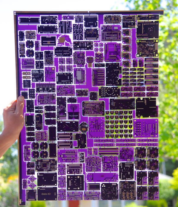
FFS I can get a pcb motherboard for that.

I think this is one of the key factors. They combine many jobs on large panels. You can look at the many video tours of PCB factories to get an idea of the size. Small jobs fill out the panel and they are willing to sell those for lower margins rather than waste the space. 100x100 mm comes from an old Eagle free limitation but has become the standard threshold for a small job.

Automation helps of course, using the Internet to take orders and computers to guide every step of the process. They run a well-oiled operation 24x7 so ramp up costs have been absorbed.

I don’t think there is much fat in PCB making now. They are diversifying into assembly, laser acrylic cutting, 3-D printing, anything that fits the Internet order mass production model.

They must have some good software to fit all those small jobs with minimum wastage.
This is why the constant demand on this forum for putting multiple boards onto a single Gerber is mostly obsolete.

It’s called a human. :wink: Have a look at a video. There are people whose job is to pack jobs on a panel. While it’s a NP problem, you can get quite far with heuristics. I think they use the obvious strategy of placing the largest boards first, then go down in size. It doesn’t have to be optimal because there are other constraints: you can’t hold up production for too long, and you may not have enough boards in a class to fill the panel optimally. They used to restrict cheapies to green soldermask and HASL but now have expanded it to other colours. Once I even saw a checkbox that allowed them to substitute ENIG or lead free for HASL, obviously to allow them to use your job to fill such panels.

While the savings on DIY panelisation are less now there are still reasons to combine designs. Home PnP and reflow soldering is one.

No it is not.
If you have an SMT PnP machine with an conveyor belt (and reflow machine after it) then big PCB’s may work one at a time but for smaller PCB’s you will need panels, and probably with “side rails” to.

2 Likes

Pooling has become the norm, it once was unusual, or often not even a thing. Pooling has obviously driven costs down dramatically. But go for a non-pooled batch (if you have very specific requirements that can’t be done in pooling), and suddenly prices go through the roof.

Of course the other factor is that those low prices come from asian companies which have dirt-low operating costs compared to western companies. It doesn’t even make sense to compare. Access to those asian companies is now very easy for everyone, a couple decades ago, it wasn’t.

Fab technology has also evolved of course, but the two above points are the main drivers IMHO.

And, you get what you pay for. You used to have an engineer to talk with when you submitted a PCB, that would give you advice, would help you get things right before fabrication and would manually modify your layout slightly to get the best results - now that’s almost all automated, and you get what you get. They are also a lot less flexible when it comes to file formats and such. You send stuff in the format(s) they list, and otherwise, no luck.

No magic there.

The Asian companies also invested hugely in automated pcb lines something western companies were notoriously slow to do.

Western pcb companies held onto to NRE to drive overall margins up or was almost always in effect a margin scam

Western companies could compete with Chinese but they get addicted to those high margins !!

JCLPcb will make more pcbs in a day that a lot of western will do in a week.

Too many western pcb favs were small under capitalised semi family businesses. It leaned towards high costs business models. The Chinese showed what automation and low costs could do to generate huge volumes of pcb business

Eurocircuits has some nice video’s about the whole process of making PCB’s, and in them you see human beings pushing a cart full of PCB’s. When you see the JLC factory video, you see PCB’s wizzing by on a conveyor belt. But to be fair, the Eurocircuit video’s are some 8 to 10 years old.

And don’t forget, what is seen in a ten second video clip, does not necessarily represent the average volume over a whole day. :slightly_smiling_face:

I think automation, that is good work flow would give a good reason. For instance JLCPCB is very strict about how BOM and other documents look. Gervbers are also checked. They wont do much manual work.

Years ago I used PCB123 (in USA) to make my boards. They were excellent to work with and would produce panelized boards (if I did the panelization layout) for no extra cost… I have no idea about their service these days as I mill my boards (only hobby stuff now).

The funny thing I just looked them up and learned they’re only 15 miles away from my house…

ADDED: I just called them - no need to use their software, they’re happy to use customer provided Gerber’s

NRE hasn’t been eliminated, it’s just absorbed into the cost (If you plot the qty vs batch cost, the intercept will be the NRE).

In addition a LOT of inspection automation has been added at both your end as the developer and especially the manufacturers. We’ve come a long way from taping up PCB layouts. That reduces the amount of labour required to check incoming files.

That leaves photostencils which are either direct printed (or the PCB is direct written) which is a lot less expensive than photoflashing it.

Then you can add production automation, volume material cost and reduced labour costs (for offshore low labour country sourcing)

1 Like

A little more remark… Many developers mistakenly think that a multilayer board is expensive and place components on both sides of the board and as a result, the installation cost increases conditionally by 2 times… Sometimes there are other problems, such as placing heavy components on both sides of the board… You always need to read the end device…