I’m pretty sure it’s not called a “ground band” but I don’t know what else to call it. In many computer PCB’s (well, at least the vintage ones I deal with) I see a ground “band” all the way around the perimeter of the board. Or even other areas of the board that is sectioned off.
On an old pcb, those look like manually placed traces. You can do that too, manually.
I’d suggest a filled zone, which is easy.
Select the desired side, then place a GND Filled Zone across the entire pcb. Where there are existing Gnd nodes, they will be connected to the zone.
If you really want a outer band, place a Keep Out area inside the Fill Zone.
Another method is to make a Footprint for it.
Making a footprint takes more time, but you have more flexibility. You can for example also make the mounting holes for the shielding can a part of the footprint and you can manipulate different layers such as the solder mask.
For the most generic use, overlapping pads are used (and a pad can be any size, just punch in some numbers) and solder mask cutout is also part of the pad definition. For examples of this, search for any footprint with the sub-string “thermal” in it’s name. Maybe it also works to directly draw graphics on the solder mask layer, but I have not tried this.
I have drawn on the solder mask layer. It works.
(shield over the 6560/6561) If you make a footprint, then do not make a part outline. This way you can put parts inside the footprint with out errors.
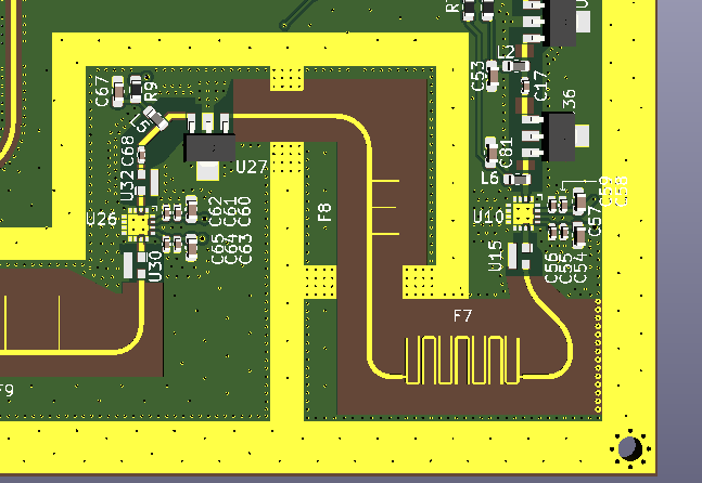
On the old board, the exposed broad traces are likely for a shield or to make contact with a metal card guide. So you need to both have copper and NO solder mask. Look at the mechanical drawings for details.
Meaning that he has to draw something in the solder mask layer in order for the solder mask not to be there (negative layer yadayadayada), I believe both of you mean the same thing with your sentences.
Solder mask is usually an inverted layer, which means the whole PCB is covered with it, except places where there are items drawn on it.
I just took a random KiCad project of mine, and then selected the F.Mask layer and drew some graphics on that layer with Pcbnew / Place / Polygon and the result is:
Good find.
I don’t use RF stuff much, but I had a look at a few of those and it confirms what I already knew. They just use SMT pads with the normal solder mask as for all other SMT parts, and in corners they overlap. Some have SMT pads with a length of 25mm.
Soon will be 10 years while I use BMI-S-210.
I like to design devices as best as I can. EMC says - contacts should be at one board edge (to avoid board currents be emitted by wires (antennas) connected to opposite edges). How to do it in DIN-rail cases where as standard you have terminal blocks at opposite edges? I decided to treat the main PCB as being edge and place at it vertical module with main (microcontroller, memories, RTC) circuits. What else you can do to make it better. You can place all of it under shield (so BMI-S-210) and add low-pas filters at each line at shield edge.
The effect of such my over-engineering is - when the lightning struck the building and all the systems with long cables went out (telephone exchanges, alarm systems, computer networks) only our access control system worked. The installer wrote to us “now everyone will earn and we will get nothing :(”
Just use (when in pcbnew) the two tool icons and draw copper zone to be filled with copper (that should be connected to a “GND net” inside the area where you draw it), such ‘copper-band’ as you name them (intended to be connected either for ESD, EMC shield or common-mode voltage constraints).
Remember to press ‘b’ key to fill/refill these copper-poor areas.
For more details refer to the KiCad user manual (pcbnew chapter), or some web tutos presenting the How to make ‘PCB power/ground planes’ (one of these https://www.youtube.com/watch?v=jEDCzisf0Rk) .
A Ground plane is a generic name for a big piece of copper connected to GND with the purpose of lowering “loop inductance” of signal tracks by offering a return path for currents. KiCad the term “zone” is used for a “plane”, (so a “ground” zone if it’s connected to ground)
In the picture from the first post, the exposed part in the center of the PCB is clearly made to be able to add a shielding can over that part of the PCB, and this makes that part a part of the footprint of the shielding can. There are several of such footprints in KiCad’s default libraries.
The other two exposed bare copper areas are at the side of the PCB, and are apparently made to connect to some form of “finger” like EMC shield or those “cushions” made from metal mesh wire. A search for “emc shielding gasket” brings up products like that: https://duckduckgo.com/?q=emc+shielding+gasket&t=hy&va=g&iax=images&ia=images
Think the phrase you’re grasping for is “guard ring”.
Guard rings are intended to stop unwanted signals from crossing the surface of the PCB. The most common usage is where you have a high impedance node and you want to avoid minute surface leakage currents creeping over the surface of the PCB. So you put a low impedance, exposed, ring of copper around the sensitive node/net and drive it to the same voltage that is on the sensitive node. In some cases that might be ‘ground’, in some it might be the output of a unity gain amplifier guarding the input of that amplifier.
Obviously in the case of shielding cans and the like a nice low impedance ground would be where you’d tie the guard ring to. Whether it is strictly still a “guard ring” is debatable, but someone ought to know what you’re getting at if you call it a guard ring.


 .
.