I have another question concerning the mask layers. Is it possible to see them in FreeCAD? I’m making an aluminum housing for the filters in the previous posts and I would like to be able to see the exposed areas of the pcb to ensure there are no mistakes. You can imagine it like this:
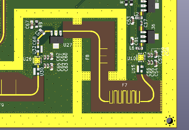
The exposed ground areas will have metal walls contact them from the housing.