Yeah… that is because of how they were created and in which order they appear in the kicad_mod file (I have no influence on that really within KiCAD).
…
(pad 6 smd circle (at 2.54 -1.27) (size 2.2 2.2) (layers B.Cu B.Mask))
(pad 5 smd circle (at 2.54 1.27) (size 2.2 2.2) (layers B.Cu B.Mask))
(pad 3 smd circle (at 0 1.27) (size 2.2 2.2) (layers B.Cu B.Mask))
(pad 4 smd circle (at 0 -1.27) (size 2.2 2.2) (layers B.Cu B.Mask))
(pad 4 thru_hole circle (at 0 -1.27) (size 1.5 1.5) (drill 1) (layers *.Cu *.Mask))
(pad 6 thru_hole circle (at 2.54 -1.27) (size 1.5 1.5) (drill 1) (layers *.Cu *.Mask))
(pad 2 thru_hole circle (at -2.54 -1.27) (size 1.5 1.5) (drill 1) (layers *.Cu *.Mask))
(pad 5 thru_hole circle (at 2.54 1.27) (size 1.5 1.5) (drill 1) (layers *.Cu *.Mask))
(pad 3 thru_hole circle (at 0 1.27) (size 1.5 1.5) (drill 1) (layers *.Cu *.Mask))
(pad 1 thru_hole circle (at -2.54 1.27) (size 1.5 1.5) (drill 1) (layers *.Cu *.Mask))
(pad 2 smd circle (at -2.54 -1.27) (size 2.2 2.2) (layers B.Cu B.Mask))
(pad 1 smd circle (at -2.54 1.27) (size 2.2 2.2) (layers B.Cu B.Mask))
)
See, they somehow managed to get in last there… although the TH’s were first and I created SMD 3,4,5 & 6 as copies from 1 & 2.
It’s really just a draw-order thing in the Default canvas though - see OpenGL for comparison:
So, you can avoid that by sorting the lines in that file into the appropriate order if it’s important for you.
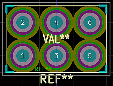
@maui …nice, looks clean.
Did you do it like that in KiCAD or was it a text-editor job (I assume the latter)?
…
(pad 6 thru_hole circle (at 2.54 -1.27) (size 2.2 2.2) (drill 1) (layers B.Cu B.Mask))
(pad 5 thru_hole circle (at 2.54 1.27) (size 2.2 2.2) (drill 1) (layers B.Cu B.Mask))
(pad 4 thru_hole circle (at 0 -1.27) (size 2.2 2.2) (drill 1) (layers B.Cu B.Mask))
(pad 4 thru_hole circle (at 0 -1.27) (size 1.5 1.5) (drill 1) (layers F.Cu F.Mask))
(pad 6 thru_hole circle (at 2.54 -1.27) (size 1.5 1.5) (drill 1) (layers F.Cu F.Mask))
(pad 5 thru_hole circle (at 2.54 1.27) (size 1.5 1.5) (drill 1) (layers F.Cu F.Mask))
(pad 3 thru_hole circle (at 0 1.27) (size 2.2 2.2) (drill 1)(layers B.Cu B.Mask))
(pad 3 thru_hole circle (at 0 1.27) (size 1.5 1.5) (drill 1) (layers F.Cu F.Mask))
(pad 2 thru_hole circle (at -2.54 -1.27) (size 1.5 1.5) (drill 1) (layers F.Cu F.Mask))
(pad 2 thru_hole circle (at -2.54 -1.27) (size 2.2 2.2) (drill 1)(layers B.Cu B.Mask))
(pad 1 thru_hole circle (at -2.54 1.27) (size 1.5 1.5) (drill 1) (layers F.Cu F.Mask))
(pad 1 thru_hole circle (at -2.54 1.27) (size 2.2 2.2) (drill 1) (layers B.Cu B.Mask))
)
The only problem I have with this: the drill size is defined in two places now and for changing it you have to change both.
I’d rather keep it in one spot only.
Do you think you could get rid of the (drill 1) part in either the front or back and still get clean results?
Like this:
…
(pad 6 thru_hole circle (at 2.54 -1.27) (size 2.2 2.2) (layers B.Cu B.Mask))
(pad 6 thru_hole circle (at 2.54 -1.27) (size 1.5 1.5) (drill 1) (layers F.Cu F.Mask))
(pad 5 thru_hole circle (at 2.54 1.27) (size 2.2 2.2) (layers B.Cu B.Mask))
(pad 5 thru_hole circle (at 2.54 1.27) (size 1.5 1.5) (drill 1) (layers F.Cu F.Mask))
(pad 4 thru_hole circle (at 0 -1.27) (size 2.2 2.2) (layers B.Cu B.Mask))
(pad 4 thru_hole circle (at 0 -1.27) (size 1.5 1.5) (drill 1) (layers F.Cu F.Mask))
(pad 3 thru_hole circle (at 0 1.27) (size 2.2 2.2) (layers B.Cu B.Mask))
(pad 3 thru_hole circle (at 0 1.27) (size 1.5 1.5) (drill 1) (layers F.Cu F.Mask))
(pad 2 thru_hole circle (at -2.54 -1.27) (size 2.2 2.2) (layers B.Cu B.Mask))
(pad 2 thru_hole circle (at -2.54 -1.27) (size 1.5 1.5) (drill 1) (layers F.Cu F.Mask))
(pad 1 thru_hole circle (at -2.54 1.27) (size 2.2 2.2) (layers B.Cu B.Mask))
(pad 1 thru_hole circle (at -2.54 1.27) (size 1.5 1.5) (drill 1) (layers F.Cu F.Mask))
)
The layout view and the 3D view look weird now though, so probably not a good idea:
Ah, need to be ‘smd’ instead of ‘through_hole’ for the non-drill pads there to make it clean again.
The order in the file is what depicts visual appearance in the Default canvas still, so the TH pad needs to come after the SMD pad to make it look nice… the OpenGL canvas doesn’t have this problem.
Just wish OpenGL would look a bit more like Default really. That green+red over each other give yellow isn’t happening in OpenGL. 


