Hi,
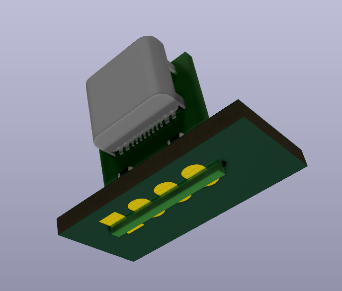
For A project I need a USB-C connector that is vertical to the main board with a specific (11mm) distance to a front panel.
The idea was to use a breakout board for the connector that fit’s into a 1mm slot and is solderes onto pads from one side.
In my first try i just made some oval SMD pads with a slot going right through them.
This is not an ideal solution as i can’t properly route to those pads (probably because the slot goes over the center of the pads?).
Also, I tried to make a little test pcb to see if it works mechanically and the manufacturer (jlcpcb) asked twice if this is really how it’s supposed to be.
What would be a better way to design those?
Also I’m happy to hear your opinion on if this mounting method is a good idea at all or if you know about a better solution.
First check the board thickness for regular manufacturers.
1.6mm is standard, and therefore probably the cheapest even though thinner PCB’s are available. Routing narrow slots can also be problematic. During routing of a slot, the mill has a side load, and it must be strong enough to withstand this side load.
It also looks like the sides of your adapter board are straight. This is OK if you use some jig during soldering (which also holds the board perpendicular. Maybe consider to add some extensions on the side to define the insertion depth.
When Routing through the pads you also depend on solder on only the top and bottom. It may be better to use the same technique as with "castellated pads, in which the pad has a plated THT hole.
Things like this beg for some communication with your PCB manufacturer, and the only way sites like JLCPCB can be so cheap is by lack of service.
Maybe you can get JLC to accept your pads if you use separated pads and keep a small clearance from the slot, so the slot is not routed through the pads itself. You can even add a little gap there. 0,1mm or 0,2 mm is probably not a big issue during soldering.
Also, placing a via through a pad makes the adherence of the pad to the PCB a lot stronger.
I have used this and it works well, it’s very sturdy provided that the pads are large enough to take enough solder tin.
Eventually there will be some DRC violation and you have to live with it.
Long oval NTPH pad; pad clearance 0.01 (or other very small value); hole size and pad size identical.
The PCB board and the oval routing have tolerances. This is meant for 1.2mm board and the slot width is 1.3mm.
THT pads with shape offset – could be SMD pads as well but the hole gives extra strength for soldering. THT works of course only if the connection pads of the other board go through this board. In your case it does.
The pad shape offset has another effect: the pad’s anchor while routing the connections is in the center of the hole and is farther from the slot edge, so it may help with the interactive routing DRC violation.
THT pads separated from the slot by a small amount. Otherwise the manufacturer may wonder if you want to do edge plating for the pads, and you don’t, or at least it’s unnecessary and complicated. They have some minimum routing/copper clearance and they may widen the gap, so be prepared and rather use their recommended value yourself. Use the solder tin to “jump” over the slot, the pads of the two boards don’t need to touch. When the pads are large enough and the there’s enough solder tin the tin forms a slope over the gap.
The good length for the slot / the other board protrusion width is a bit random. Most probably you want to add some length to the slot and manually move the other board in the slot so that the pads are in their places. I have assembled these by dozens and it was easier to find a value where I could just push it there and solder. You can also leave it tight and if necessary use a file for the other board edges.
I believe you used a large oval pad and put the slot through them. That is a problem because the connection point is in the center of the SINGLE pad.
You need 2 Pads per connection as shown by eelik above.
I suggest the tiny pcb with the usb conn be wider then have a shoulder where it narrows down before going into the slot. That way you just insert the tab in until it hits the shoulder stop. <-- Did that make sense?
Using through hole pads or vias to make the pads more mechanically stable seems like a good idea.
Yes, this makes perfect sense. I don’t think it’s absolutely necessary in my case because i will solder the board after mounting the front panel that has an hole for the usb-c connector and should hold it in place, but it still might make assembly easier.
I went with 1mm because it’s not more expensive and the usb-c connector is intended to be used with thinner boards. soldering it to 1.6 is possible, but not ideal.
They actually accepted it but asked if this really is what i want - which delayed my order for two days. I’m still amazed that at this price an actual human takes the time to ask me about a my order…
I will implement some of your ideas and share what I come up with here in case anybody is interested.