Hi, this is my first post and I joined the community because I need help with a project layout.
I own a quite large collection of Nintendo Game & Watch machines and I restore a lot of them. One of the common problems in the multiscreen versions is the ribbon cable. Do to the ageing and wearing, the traces tend to broke or the conductive surface of the traces tend to disintegrate. This ribbon cables can’t be found anywhere and ones that are available are old ones removed from broken machines with the risk of failing because of the age.
I came out with an idea and found out that someone already has it and it’s to make a ribbon cable out of FPC/FFC. More reliable and durable.
I can’t put here the images because I’m a new member so I paste a link: old
I want to make a design layout to generate the gerber file so I can send it to pcbway.com to manufacture it. But I don’t really know how to achieve that. I first tried to create my own foot print and then draw it on the board editor, but I don’t know how to configure the layers and how to do the holes and traces. I also thought about create a DXF file in FreeCAD over the scanned original image and then import it to KiCAD but once again don’t know how to do it.
I think is a very easy work for a trained user but for me is a total riddle. I’m asking here if some one could help me doing it or at least give me some step by step tips so I can do it by my self.
A Symbol for the Mounting holes (or for whatever this holes are).
A Footprint for the connector?
A (unfinished) layout?
I suggest to draw all the copper on the F.Cu layer. The outline should be on Edge.Cuts and the holes should be NPTH.
You should add a F.Mask where you have the connector, as part of the Footprint. That means that there is no Soldermask where the connector is.
So, finally I managed to do the following as johannespfister mentioned:
Create a Schematic
Add a Symbol for the connector
Add a Symbol for the Mounting holes
Create a Footprint for the connector and associate it to the symbol
Create a layout
All the copper is on the F.Cu layer. The outline is on Edge.Cuts and the holes in NPTH.
As for the F.Mask, I’ve checked that is no solder mask in the connector pads, but there is in between of the pads. Is it possible to draw a custom F.Mask?
Yes. When you create a footprint and place a pad, you can select in the pad settings if F.Mask should be applied or be kept unchanged. And you can draw primitives on F.Mask, if you draw something on F.Mask there will be no solder stop lack there.
I’d be a little worried about the reduction of width of the tracks from the contact pads to the covered track section.
In the original picture you showed the width of the two are the same.
In general, when you have flexible stuff, sudden changes in width and sharp corners tend to be prone to breakage due to stress concentration. If you really don’t want wider tracks, at least make a smooth teardrop which is significantly longer than the contact surface width.
Similarly, when you go around the holes you may need to reduce the width of the tracks slightly in case you use wide tracks, and there the transition in width should be gradual and smooth for best longevity of the part.
Not all PCB fab houses can make Flex.
Those that can will have requirements.
Here’s link to one often used by folks at this forum (and snippet of page, below) (Flex PCB tab selected)
In Kicad, click the Green Icon to edit Board Setup where you set values needed…
It’s just another circuit board. The traces are fairly wide, and end up in solder pads on each end.
No need for new footprints.
Then when you’ve rechecked the dimensions, submit it to a board fabricator that does flexible boards. You might think about niceties like plating the contacts.
It’s one layer.
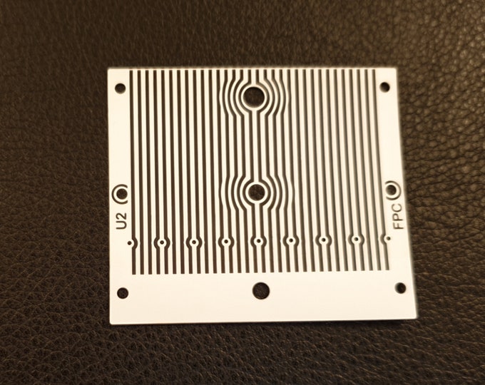
Ok, so I think I’m ready to go to production. Here is the final FPC and I ready generated the gerber files and uploaded them to JLCPCB and everything seems to be fine.
As much as can be told from looking at the images . . . . it looks OK, are you happy that the thickness is OK ? it needs to fit properly into the connector(s)


