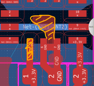
I added a GND filled zone surrounding my entire 2 layer PCB, for both the top and bottom layers. However, despite being of the same net as the pins I’m trying to connect, it doesn’t fill the area between them. I can even connect the pins with traces closing off the area by the intended net, and it still doesn’t fill it, just makes this weird blob:
I’ve tried adding a smaller, higher priority filled zones, but they just draw the same blob in the restricted area (can’t show it because I can only post one image).
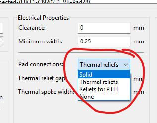
I’ve also tried changing the connection to copper zones of the pins 6 and 7 to both thermal relief and solid, to no avail.
Any way I can fix this? Thank you in advance!
What kind of Pad connection have you set for your filled zone ?
Hello sir,
I had it set as Thermal reliefs. After your question, I tired all other types, and none of them resulted in that area being filled, though other areas (besides the pad connections) were affected.
Should be solid if you want it fully filled . . . I assume you remembered to ‘B’ - refilled zones after each change ?
Next step is to check all your clearance settings . . .
I apologize for the delay in my reply. I can’t reply very quickly since I’m a new user.
The image I’m sending now shows how it looks with solid (I did remember to press B)
I’m sorry, but I’m unsure what are the relevant clearance settings in this case. Could it be these?
Changing the minimum clearance from 0.2 to 0 shows no effect.
1 Like
Not sure why it’s enforcing what looks like a large clearance . . . it may not be that large, it’s hard to know for sure without knowing what all the footprints are.
Select this pad and this fill . . .
Then go to Inspect, and click Clearance Resolution
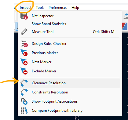
It should tell you what the clearance is and what is determining that clearance.
Thank you! The problem was the clearance setting in the Filled Zone feature.
1 Like


