Hi,
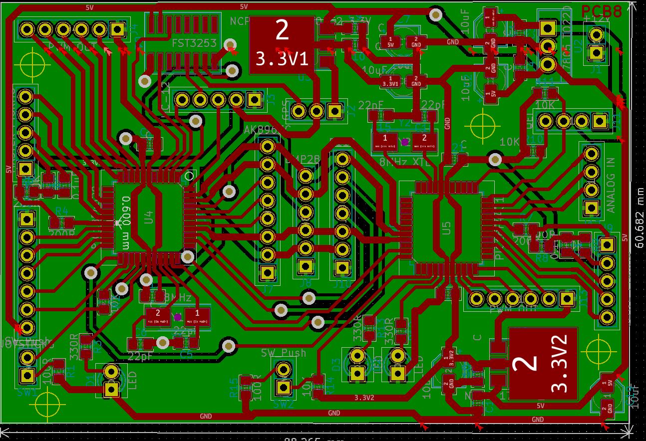
I’ve just updated to V 5.1.12, and almost finished a PCB. I carried out a DRC test which was ok, but I tried again today, and got this, where all of the arrows report ‘too close to edge’.
Can anyone explain please, as some are obviously not near the edge.
Camerart
Is the design confidential, can you zip the project and attach it here?
Your Edge.Cuts layer which should describe the board outline is wrong. It has some marks but not outline. The DRC messages are problematic in themselves and I would consider this as a small bug – they are far from any Edge.Cuts graphics – but fixing the root problem should help.
Below are the properties of the line on the “north” side of the PCB.

The line should have been on the “Edge.Cuts” layer (which should be obvious after following eelik’s links.
I also noticed the “weird” coordinates.
If you set the grid to something coarse (for example whole millimeters) then it is easy to both make your PCB rectangular and with rounded numbers for their size.
Just curious:
Have you thought about adding some mounting holes to your PCB?
Hi e,
I think the extra marks are measurements I added.
Ok, a bug, I can ignore the arrows. Fixing the root problem? Who does that?
C
Hi again e,
I looked at the layers, but I’m not sure what I do now?
I’m using 5.1.12
C
Hi P,
PCB making is not easy for me, so I usually need clear instructions what to do!
Which line should be on the “edge cuts” layer, As you can see it wasn’t obvious. (Perhaps when I’ve read it 5 more times it may become that  )
)
I have set coordinates before years ago, but this time is the forst timeI have exported the gerber etc files including the DRL file. I have always bee interested in XYZ plotting, and noticed the difficulty with my coordinates, so I did set it, but perhaps after I posted the ZIP.
Mounting holes will come later when I try to fit the PCB into the transmitter, I could probably use the alignment marks, once I get them right.
C
The root problem is the missing outline. You add it by drawing graphic lines to the Edge.Cuts layer. The lines must form a continuous polygon. Endpoints of two lines which form a corner must match (there’s only one x,y coordinate for a corner), there must not be space between them or they must not go past each other, and the polygonal shape must be non-intersecting. You also have to move the extra marks to some other layer, for example Drawings or Eco.
You probably want a rectangle and you can draw it with the Rectangle graphic tool. The rectangle shape is automatically translated to lines when you draw in the Edge.Cuts layer.
Hi e,
Clear instructions appreciated
As mentioned the outline was in the drawing layer, and I noticed the fact that the outline was white, where it used to be yellow, but it passed me by. It is now yellow.
I think that now the outline is correct, the arrows have gone, so perhaps this was the answer?
I removed the alignment targets.
Thanks, C.

This topic was automatically closed 90 days after the last reply. New replies are no longer allowed.