I’ve cropped your screenshots a bit and post them here on the forum.
(As an automatic anti spam measure, you have to gain some “experience” before you’re allowed to post pictures here)
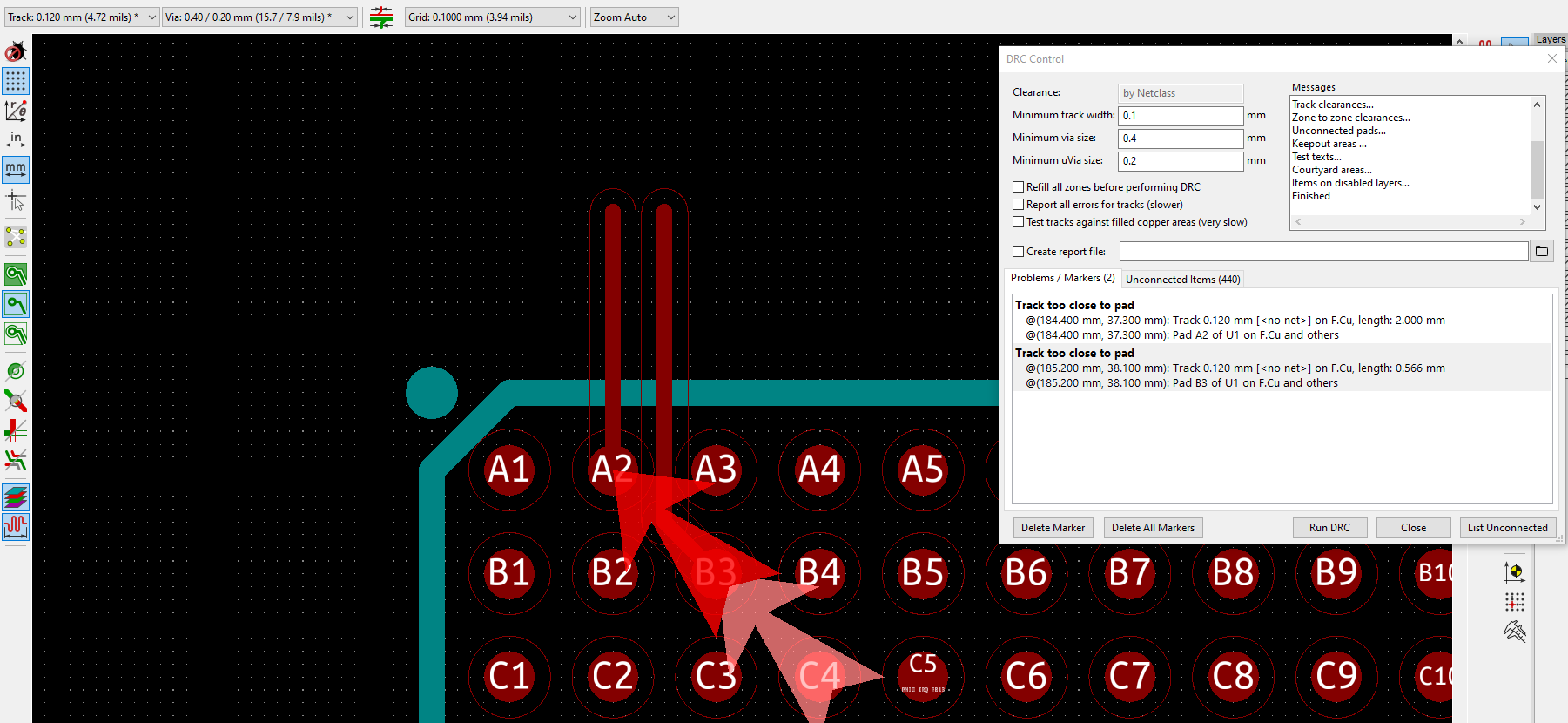
I am a bit confused what is going on here.
Both tracks are [< No Net>] according to the DRC:
And all the pads of your BGA are likely also not part of any netlist.
If a pad is part of a netlist then (with the default settings) the name of the net should be listed below the pad name, like in this THT Footprint:
(Note the text: “Net-(U2-Pad22)”, which is an automatically generated net name, and the white ratsnest line that shows the pad is connected to some other pad (off screen).
The BGA does have a name U1.
“No net” copper tracks should connect to pads that are not in a netlist.
But the obvious thing that is missing here is the netlist.
How did you get to this stage?
Did you do these steps:
Draw a schematic.
Assign footprints to schematic symbols.
Eeschema / Tools / Update PCB from Schematic [F8].
On a side note, working with a BGA with 289 pads is not a good way to learn KiCad. Beginners are bound to make simple mistakes, and repairing such mistakes on high pin count parts is a lot of tedious work. To get to know KiCad, schematics with 10 to 20 parts, and a total of up to around 50 pads are ideal. Such schematics have enough complexity to experiment a bit with the way KiCad work, while mistakes are still relatively easy to fix.
The schematic is made, not all the footprints are done yet but the connectors, caps,resistors and all the main components are on there. Some are left for later as i’ll have to see whats available for the inductors/crystals.
Clicking the traces shows me net C11 and net B23.
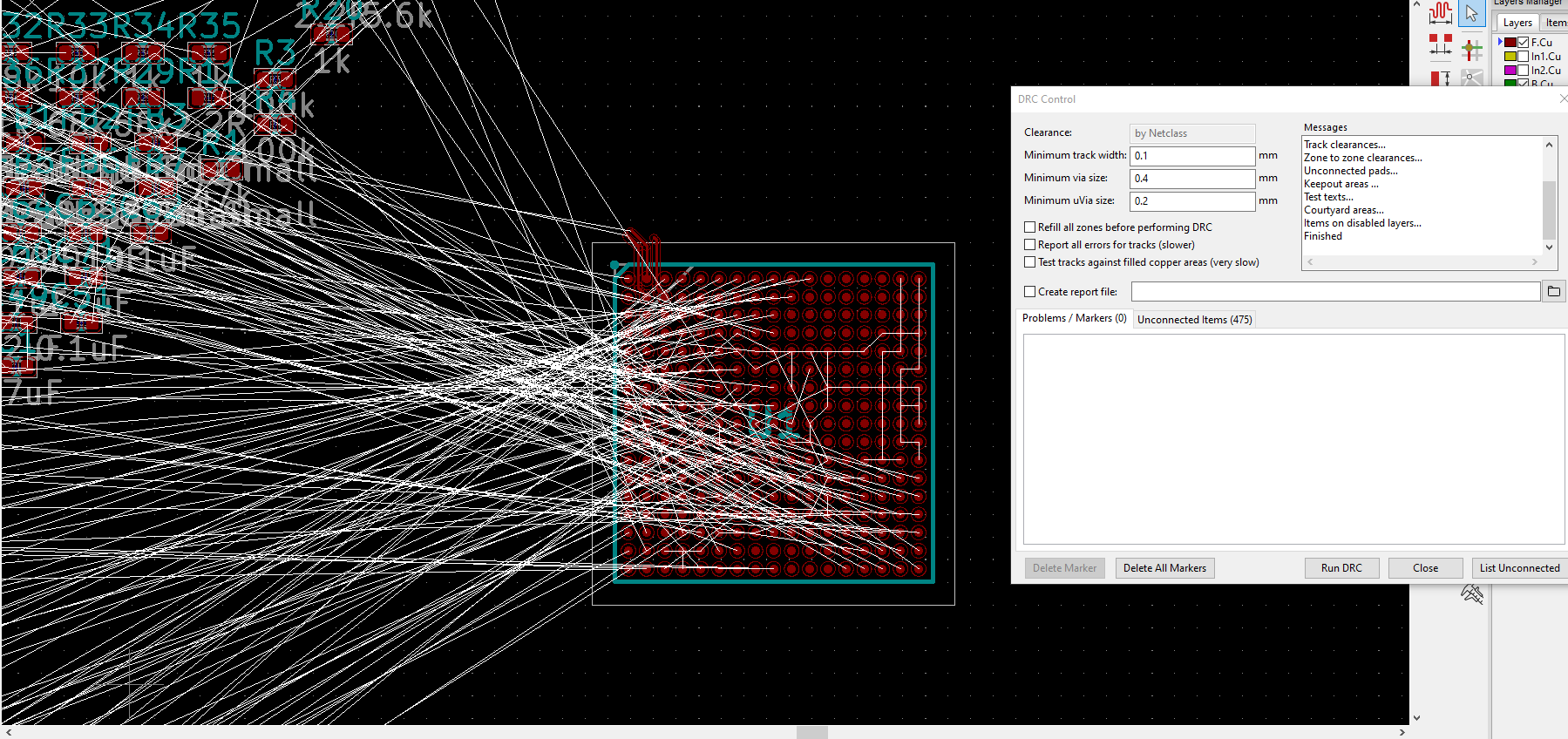
As you pointed out the missing airwires are odd. So i’ve made a new PCB schematic, deleting the old one and now they do show, and the DRC errors are gone. Odd as the traces are still the same.
I thought that perhaps it was something i accidently turned off but it seems to have been an issue with the file.
EDIT: as a reply to learning kicad, i’ve made 5 4 layer boards so far with no real issues, so i appreciate the concern but the actual design is pretty simple. It’s just a board to break out the pins with the needed power sources and some decoupling.
Normally the schematic symbols and the PCB footprint are matched with a “timestamp” (In KiCad V5.1.x) or UUID (In KICad-nightly V5.99)
Just adding a part to the PCB and calling it “U1” does not match it with the “U1” in the schematic (by default).
To use the Refdes as match method between Schematic symbols and PCB footprints you have to use: Eeschema / Tools / Update PCB from Schematic [F8] / Match Method: Re-associate footprints by reference


