Differential pair not exiting pads correctly

Trying to do some MIPI DSI layout, but when I try to exit the pads, the router freaks out and places some extra trace to the right, when I’m exiting left:


Trace width, trace separation = 8, 8 mils
Any idea how to fix this? I’m still very new to kicad, but have done a lot of work in Eagle

It’s worth noting that it does the opposite if I try to exit right instead of left:

What is your kicad version? (help about kicad -> copy version info)

Apologies, version info:
Application: KiCad
Version: (5.1.6)-1, release build
Libraries:
wxWidgets 3.0.4
libcurl/7.66.0 OpenSSL/1.1.1d (Schannel) zlib/1.2.11 brotli/1.0.7 libidn2/2.2.0 libpsl/0.21.0 (+libidn2/2.1.1) nghttp2/1.39.2
Platform: Windows 8 (build 9200), 64-bit edition, 64 bit, Little endian, wxMSW
Build Info:
wxWidgets: 3.0.4 (wchar_t,wx containers,compatible with 2.8)
Boost: 1.71.0
OpenCASCADE Community Edition: 6.9.1
Curl: 7.66.0
Compiler: GCC 9.2.0 with C++ ABI 1013

Build settings:
    USE_WX_GRAPHICS_CONTEXT=OFF
    USE_WX_OVERLAY=OFF
    KICAD_SCRIPTING=ON
    KICAD_SCRIPTING_MODULES=ON
    KICAD_SCRIPTING_PYTHON3=OFF
    KICAD_SCRIPTING_WXPYTHON=ON
    KICAD_SCRIPTING_WXPYTHON_PHOENIX=OFF
    KICAD_SCRIPTING_ACTION_MENU=ON
    BUILD_GITHUB_PLUGIN=ON
    KICAD_USE_OCE=ON
    KICAD_USE_OCC=OFF
    KICAD_SPICE=ON

Send us a stripped-down version of the board. What’s the router mode you’re using? (shove, walk?)

Tom

I worked around this issue by just finishing the routing single ended, but attached is the whole project. All router modes exhibit the same behavior.

OSSW_Eval.zip (809.6 KB)

I had a quick peek at this, and behaviour is the same on my Linux box.
I will do some experiments if I can narrow it down to some setting in KiCad and report on that later.
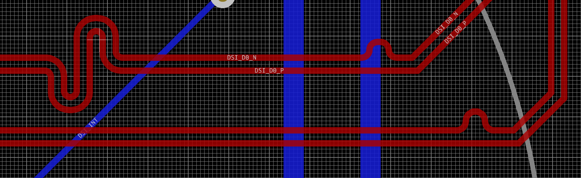
But for now:
Differential routing is not only about length matching.
It’s about keeping signal integrity along the whole path, and 2 runners running along the differential tracks with the same speed should be as close together as possible along the whole way.

Here you introduce a length mismatch for no apparent reason. If you want to use via’s here, then place them vertically, and exit the traces horizontally.

image

Same here.
An unavoidable length mismatch is created in the corner, and the camel bumps compensate for that, so the camel bumps should be as close to the corner as possible.


The location of the S-curves is irrrelevant, as they affect both traces of the pair in the same way.

Note that the top camel bump is bigger than the bottom one.
This is probably to compensate for the length difference you introduced by misplacing the via’s, so you have skewed signals all the way from the via’s to the camel bump. Yuch!

I’m not an expert on this, just parroting from memory some stuff I read about signal integrity.

I also think via size matters, and via’s (in differential pairs) should be small and also have minimal annular rings.

Although, they are 0.8mm and 0.4mm drill which may make manufacturing an issue if you go much smaller.

Application: Pcbnew
Version: 5.1.6-c6e7f7d~87~ubuntu18.04.1, release build
Libraries:
wxWidgets 3.0.4
libcurl/7.58.0 OpenSSL/1.1.1 zlib/1.2.11 libidn2/2.0.4 libpsl/0.19.1 (+libidn2/2.0.4) nghttp2/1.30.0 librtmp/2.3
Platform: Linux 5.4.0-42-generic x86_64, 64 bit, Little endian, wxGTK
Build Info:
wxWidgets: 3.0.4 (wchar_t,wx containers,compatible with 2.8) GTK+ 3.22
Boost: 1.65.1
OpenCASCADE Community Edition: 6.9.1
Curl: 7.58.0
Compiler: GCC 7.5.0 with C++ ABI 1011

Build settings:
USE_WX_GRAPHICS_CONTEXT=OFF
USE_WX_OVERLAY=ON
KICAD_SCRIPTING=ON
KICAD_SCRIPTING_MODULES=ON
KICAD_SCRIPTING_PYTHON3=ON
KICAD_SCRIPTING_WXPYTHON=ON
KICAD_SCRIPTING_WXPYTHON_PHOENIX=ON
KICAD_SCRIPTING_ACTION_MENU=ON
BUILD_GITHUB_PLUGIN=ON
KICAD_USE_OCE=ON
KICAD_USE_OCC=OFF
KICAD_SPICE=ON

Ah, as you can tell, I’m certainly new when it comes to differential routing. They are placed at a 45deg to each other because that’s what Kicad did automatically when I went up with the route. I had to go up though because otherwise the vias would overlap with the clk pair below. Should I go higher with the vias so they’re one above the other, then do 2 45deg shifts to get it down?

Yeah, I was thinking about that as well, but I was super unfamiliar with how kicad was placing the camel humps, so I was just happy to get them placed down at all. I’ll see what I can do about moving them.

Thanks for your feedbakc!

About the corner:

  • Start differential pair from the pads.
  • Click on the board to make the first corner.
  • Press V to start via placement.
  • Move mouse just far away enough to add horizontal stubs.

image

Another small thing.
A track segment is missing in SPI_MOSI, and it is reported by the DRC. You probably noticed this yourself though.

I tried to copy your suggestions:

and

Is this better? I’ll look into my fab’s capabilities for reducing via and annular ring size

Yeah :smile: it got deleted accidentally as I was ripping up stuff, it’s back now!

Yes , that looks more like it.
Most Ideal place for the camel humps is probably in the 45 degree section itself though.

Also:
halfway the S you have skewed signals, and the S could be avoided altogether by adjusting your via placement.

I may well be nit picking here. Things like this become irrelevant if the errors introduced by skews are small enough. “Small enough” is a function of frequency content. This may only be relevant for multi GHz signals (rise time is the important factor)

For info far exceeding my own knowledge do a bit of reading in something like:
https://html.duckduckgo.com/html?q=differential+pair+routing+signal+integrity

You’ve got plenty of GND and via’s on this board (Though I am not sure if those GND vias all over gain you much).

For signal integrity though, you should place via’s as close as possible to connector and IC pins. Among other places, for you this means pins 4, 10 and 16 of CN2.

I’m not familiar with these connectors, Pins 25 through 28 may well be only mechanical. If they are connected to a connector shield, then also place via’s near them.

I think I found it.

CN2 has a pitch of 0.4mm, and you have your differential pair set up for 0.2032mm

If I set both the differential pair with and gap to 0.2mm the weird extra parts are gone.
Pcbnew / File / Board Setup / Design Rules / Net Classes

It even becomes more clear if I run a differential pair to CN2 instead of from it.
KiCad maintains the 2.032mm gap untill the center of the pads, ten adds the extra parts to make up for the difference right outside of the pad clearance on the “other” side.

Arguably, KiCad should not even route a differential pair here at all, since specified clearance values can not be met.

CN1 has a pitch of 0.5mm, and is therefore wider than the differential pair spec. and has no such issues.

3 Likes

Ah, I see now. Without knowing the internal code behind it, I was looking at what it did on CN1, and assumed it would apply to CN2. On CN1, it extends the pair out of the pads at the pad pitch for a little bit, then begins respecting the specified clearance. I figured that it would again ignore diff pair clearance rules for a little bit (since my actual clearance limit is 6mils) and then spread out as it exited CN2.

If I may make a suggestion, I believe this should be the implemented behavior; or as you suggest, it just doesn’t route it at all.

Thanks again for all your help :slightly_smiling_face:

If anyone is interested in improving KiCad’s behavior in this regard.
I’ve made a simplified test project out of it that still has this behavior.

I can see 2 ways of improving:
1). KiCad refuses to route because clearances can not be met.
2). The gap with adjustment is done on the same side as the tracks go to, in the same manner as with CN1, where the pin pitch is bigger then the differential pair settings (Gap + Width).

I did not find an issue about this on gitlab.
Would this case be worthy enough of such an issue?

The PCB now looks like:

CN2 (Left) has “weird” extensions, while CN1 splits the pair to a wider gap before attaching to the connector.

[Edit: Also removed STEP files. Zipped project is now 13KiB instead of 800KiB]

OSSW_Eval_Differential_Pair_Anomaly_2020-08-10.zip (13.6 KB)

1 Like

This topic was automatically closed 90 days after the last reply. New replies are no longer allowed.