Hello everyone, final changes.pdf (78.0 KB)
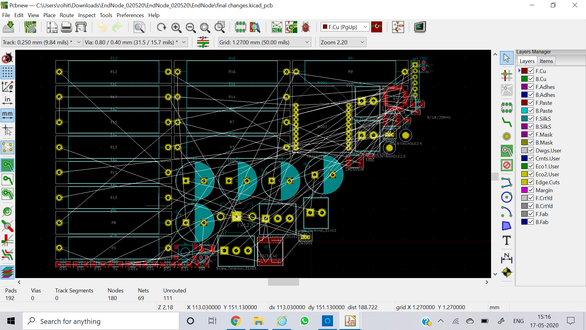
This is the finalized schematic for my project. I have now finished assigning the footprints and uploaded the netlist too. This is how the screenshot looks now.
Since this is the first PCB I am making, this looks really intimidating to me.
So can someone tell me some useful tips on how to start the PCB design. I know the basic steps like first rearranging the components to prevent crossover then drawing the traces etc.
I have seen some videos of shawn hymel already , any other relevant sources or tips might be helpful
If you know your board dimensions, lay that out first on the edge cut layer. I like to work the schematic and PCB in parallel so I don’t end up with this situation.
I do usually start to design small functional blocks, and then try to arrange them the way that seem optimal to me. Like e.g. if I do have an opamp application, or power converter, lay the necessary components and then arrange them on final board.
I try to check components manufacturer’s papers to use recommended application design as a starting point.
I have the advantage that te circut design is mine, so I know which part belongs where. If what you get is just the netlist and parts, things get more complicated.
This project is too complicated to be ideal for a beginner.
I guess that between 10 and 20 footprints would be ideal.
Very simple projects do not give you enough opportunity to experiment with KiCad’s features, while a too complex a project ends up in tedious work to repair things for errors you are likely to make, and realize too late. For example, those resistors look awfully big to me, and you have probably chosen the wrong footprints for them.
There is nothing wrong with building a first PCB in KiCad without any intention of really producing the board. I believe it’s even an advantage, because you can focus more on how the process works and less on board size and other details that are only important for “real” PCB’s, but not relevant for learning KiCad’s work flow.
Zooming in and out of stuff in KiCad is a great feature, but it makes it very hard to get a sense of how big things will actually turn out to be in real life.
Almost 3 years ago I made very simple tutorial for test fitting footprints. There are more “advanced” methods to do this, but the method I described is too simple to skip.
When you print out the PCB you also see how big all Footprints actually are.
You can also add a measurement gauge to the PCB as a size reference. Pcbnew / Place / Footprint / {click in black area} / {in filter type:} gauge
and then select a gauge you like.
Open at the same time schematic and PCB. When you move any element at PCB it is selected at schematic. Group elements according to schematic. Groups far away one from another.
Arrange elements in each group looking mainly at connections needed to be done.
Make these connections in each group.
Place groups next to each other.
Make unrouted connections.
Make Edge.Cuts around all elements.
I am designing PCBs letting all bottom layer to be continuous GND. To not see GND wires while moving components I remove (text editor) the GND net from netlist at the beginning of placement process.
The ability to filter nets for ratsnest display might be a nice feature (to quickly remove all ratsnest wires for connections made to board planes further down the road).