Curved tracks / free form drawing

I am new to KiCad born from the fact that I need a flexible PCB to repair a lens. I have drawn the board and added footprints but somehow I cannot draw tracks.

For one I cannot find how to draw round tracks. even when I start drawing from the 10 pin connector at the bottom of the board the line does not even keep straight but jumps all over the place.

The narrow part is only 5.5mm wide. The layout a super simple! I could draw the tracks in any program but need a format I can send to OSH Park…

Is this possible in KiCad? Or should I use another program? I hope someone can help me out!!

KiCad|689x486

Thank you!

David

As far as I know it is not possible to draw round tracks with KiCAD at the moment.
A working solution could be using a filled zone instead of a track or create a matching “footprint” formed as intendet to be used as track. How many parallel tracks do you want to use?

Timo

It is 7 parallel tracks, Maybe the footprint option would work…

Change interactive routing settings to highlight collisions mode and tick free angle mode, you can now lay down in whatever angle you please, do this to approach a curve with segments and your done, had to do this method for quite a few really compact boards to get everything to fit nicely.

3 Likes

Thanks for the tip. Somehow that does not work on my layout, I probably have still a setting wrong but the tracks start spreading all over the place…

Your boards look great!

As far as I know KiCad does indeed not support arc’s in tracks (yet).

What is supported is drawing arc’s on non-copper layers, and making pads from graphic items in the footprint editor.

Super mini tutorial.
1). Open the footprint Editor.

Footprint editor / File / New Library / (Enter name) / [Enter] / Add to Project libary table.
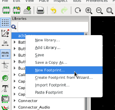
2). Select your new library by double clicking on it, then [RMB] & “New Footprint” from the popup menu:
image

3). In your new footprint in the footprint editor draw something like:
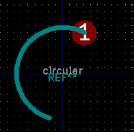
image

Notes:

  • I drew the arc on the silkscreen layer
  • You can adjust the widht of the arcs by hovering over them and press ‘e’ to edit.
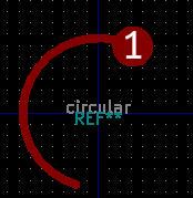
  • It must have an pad which becomes the attachment points for further tracks.

4). Draw a box around your arc and pad, then [RMB] and select "Create Pad from Selected Shapes. Your silkscreen arc has now become part of the pad.
image

5). If you draw a box from upper left to lower right, then items crossing the box are not part of the selection. However, if you draw the box from lower right to upper left, items crossing the box boundaries are included.

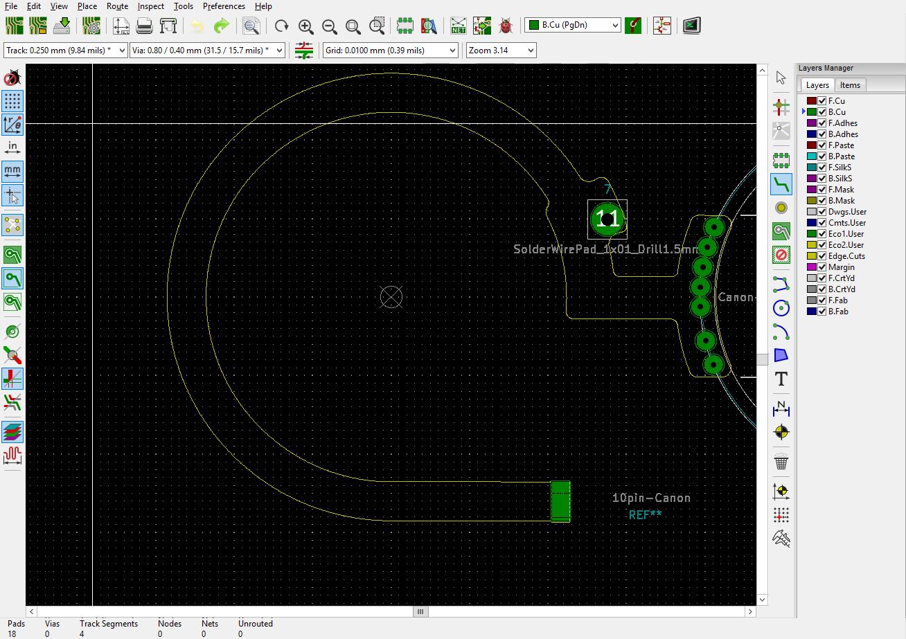
6). You have to repeat this for every arc, and then it becomes difficult to select the next objects for the custom pads. It is a lot easier if you move the custom pads to the other side of the board after drawing, and then hide that layer while drawing the next custom pad. You can select the layer by hovering over a part of the pad and then press ‘e’ for edit, and select another copper layer. You should also remove the ticks for the mask and paste layer, because you do not need these.

7). The next limitation you have to work around is that your circular footprint only has an attachment point on one side. Resolving this in a way that would not generate DRC errors will be difficult, but also not very important on such a relatively simple PCB.

It is possible to draw real arcs this way but you have to work around some limitations in KiCad which make it a bit difficult.

The way Rerouter suggest is also possible, and quicker, but you will not have real arcs, and you indeed have to disable the push and shove of the Interactive Router or it will create a big mess.
Drawing the Arc tracks by hand is a lot more accurate and easier if you first draw circles on the Dwg.User or another “technical” layer, and use those as guidelines to draw your semi-arc track segments.

1 Like

Thank you for the comprehensive explanation! That should work as it is only 7 tracks and this part potentially saves me a £400.00 ($600.00 US) repair!

Thanks again!

1 Like

This may be a known bug which will be fixed in 5.1.3.

1 Like

If you have a launchpad account, you can click the “this affects me to” on the top.
The current counter is on 46, and arcs in tracks are on the roadmap for KiCad V6.

https://bugs.launchpad.net/kicad/+bug/1577958?comments=all

Also, if you have CDO ( = OCD spelled alfabetically as it should be) then you can look into the “net tie” footprints as a workaround to draw a pad on both ends of the ARC without generating DRC errors.

I’m also curious as to how this Flex PCB is to fit. It looks like it goes inside the lens of a Canon camera. Does the flex PCB move with zoom / focus, or is it just fixed?
If it does not move, you could strip a part of the flex and solder laquered 0.2mm wires to it, with a dab of glue on the most fragile parts. If it constantly moves this is not a good idea.

I’m also curious about the cost of a single custom flex.

1 Like

I’m using 5.1.2 if it matters,
routing%20settings

you draw the trace bit by bit instead of just dragging to the end
you can then draw over corners to smooth it out

It proves to be very frustrating I have drawn the PCB in the footprint editor but when converting to pads the curve are really randomly broken up… This is of course small but why is it such a problem to have the capability of the pad designer in the tracks…From this:

To this:

Will I have enough clearance these 7 tracks are together just over 5mm wide…

This is a Flex from a TS-E lens and this accommodates the 90 degree axis change. That means it is dynamic. The connector is static bend 180 degrees but halfway it comes back on itself with a 180 degree which moves over a 90 degree section, in about a space of 3mm. Soldering is not an option.

Shame that Canon decided to discontinue this flex and just sell the whole shift part including Main PCB and rack and pinion gearing.

the Custom flex should be about $40 then you get 3 including postage…

1 Like

KiCad has come a long way in a few years but it still has a number of areas where it is weak or features are missing unfortunately.

Can you zip your project and post it here?
I would like to have a close look at it to see what I can do.
A few things I (or you) can try is to make a gerber of your first nice arcs (though the are a bit unevenly spaced???) and then look at the gerbers.

If the arcs as being graphical objects work, then a workaround is to draw the whole thing on silkscreen and then change the file names so “silscreen” becomes a copper layer. But this is a very ugly workaround.

It may be possible to do something with FreeCAD and the StepUp plugin, but that is a route I would not reccomend to a beginner,nor am very keen on myself, because my experience with Stepup is very limited.

Just had another Idea that can give quick and easy results.
As an experiment I drew a single track segment and created an array out of it.
(Right click / Create Array / Fiddle with the coordinates.
Made a screenshot of it with (purposefully) too short tracks to try if it works. And it works as expected.
Fiddling with a bit of math to get the coordinates right is pretty simple.
image

The most important caveat would be to get the endpoints to match close enough (or purposefully overlapping a bit) for DRC to be successfull.

If you go this way, then disable the “push and shove” of the interactive router:

Pcbnew / Route / Interactive Router Settings / Mode: Highlight collisions.

You might find it easier to draw the layout using a drawing program - eg FreeCad and exporting a DXF of the copper layer. You can then import the DXF to the relevant copper layer in Kicad. The disadvantage of this is that there is no ‘functional connection’ as far as Kicad is concerned - and the ancillary component on either end will appear unconnected for DRC. In a more complex circuit, this might be problematic but if I understand correctly, you simply require a curved flex pcb with a connector on either end and you simply require tracks and no pads on this section of the pcb. You might have to force the connections to ‘real’ tracks.

I ended up doing something similar in this project. Originally I used >180º arcs but had some problems with running them through a panellise so substituted <180º arcs and haven’t really tidied them up properly.

45

Thank for your feedback. I designed it completely in the footprint editor but now get stuck as the parts which are not converter to pads stay on the eco1 user layer I put them on. I guess I will take your approach!

It is indeed 2 connectors 1 soldered to the flex the other just plugs in a connector and a couple of fixing holes with a copper pad.

Do you know if I can I also upload a solder mask in that way as I really need everything covered except the connectors?

Making cutouts in the solder mask would be easy with a simple footprint.

I also wonder how you made your board outline.
Drawing it in KiCad would have ben excruciating, and I assumed it was also a DXF import.

I also noticed that the bottom part of your Flex is not horizontal, while I assume it should be. This could be an indication there may also be other errors in the board outline.
image

KiCad’s 3D viewer is pretty fussy about faulty board outlines. Can you see the PCB in the 3D viewer? (Shortcut key: [Alt + 3]).

1 Like

Yes and no, I did it the excruciating way in KiCad! And that line it is at 0 degrees but there is indeed a lot of play between 0 and -180 degrees and I picked up on the step in the line but it depends on what the zoom level is.
This is how far I got but cannot progress…

.

1 Like

@David_Bleeker, would you mind to share the fp?

Not sure even how, or what use it would be as this is at the moment just pads on a copper layer and the tracks are just drawn on a user layer. But as soon as I start merging these they do not stay round as shown earlier in the thread and come to close for comfort.

If you share the design then I (and others) can have a look at it to try some things.
Sometimes I get better ideas while experimenting with silly ideas.

Just now I had an idea that is a variant of the array I posted earlier.
What I did was to create an array just like before, but with the segments rotated 90 degrees, so the track segments resemble a clock face.
Then one by one you can hover over the outside of a loose segment, pres ‘g’ to drag the enpoint, and then snap it to the inside point of the next track segment.
This wil give you a pretty decent circle, depending on the number of segments.
The work itself is a bit tedious and boring, but it is pretty simple to do.

Next thought was to only draw half or a quarter of a circle, (or 1/8th) and then use copy and mirror to extend it. But it’s not needed.

You can use one of the re-oriented track segments, and then create a new array out of it. With a circular array, the amount of effort does not increase with the amount of segments. Drawing your 3/4 round arc with an array of one degree increments is really close enough to not even be able to see the segments.

Something similar is done in the Skidl Clock example, but there the array for the circular tracks are made by a script.

If you do not like this approach, please say so instead of just ignoring my posts.
If so, what are your objections?

2 Likes